Gan Hemt Fabrication Process
GaN can be deposited on several types of substrates such as Sapphire, Silicon or Silicon Carbide (SiC), but the cost of GaN epi process and repeatable high-quality crystal growth are challenges in GaN-based device fabrication.
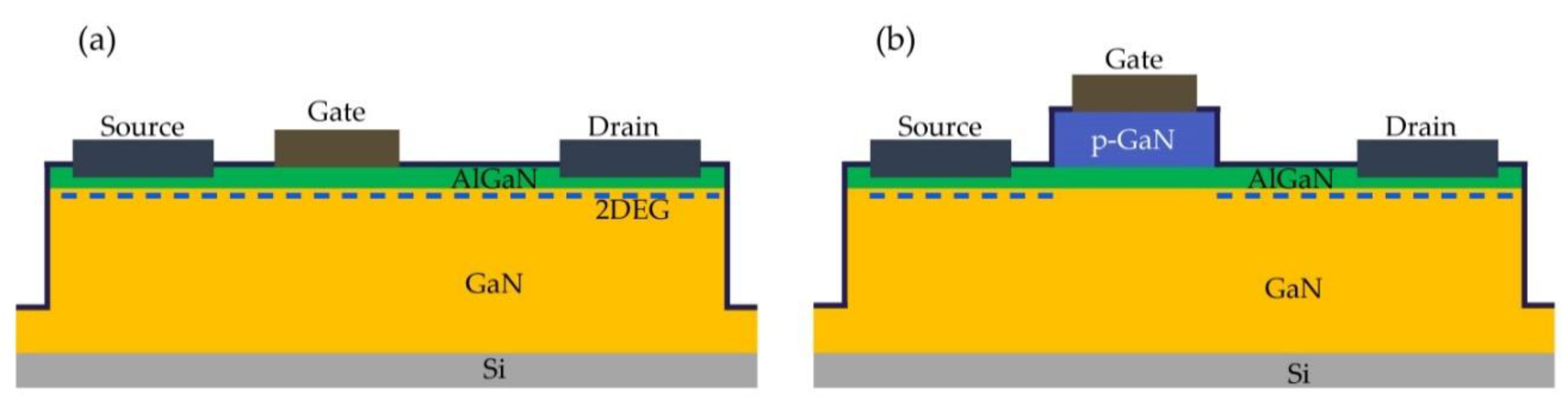
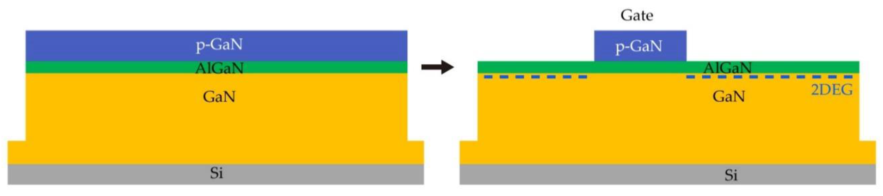
Gan hemt fabrication process. Effects of p-GaN gate structures and fabrication process on performances of normally-off AlGaN/GaN high electron mobility transistors Takaaki Kondo1*, Yoshihiko Akazawa1, and Naotaka Iwata1,2 1Advanced Electron Laboratory, Toyota Technological Institute, 2-12-1 Hisakata, Tempaku-ku, Nagoya 468-8511 Japan 2Research Center for Smart Energy Technologies, Toyota Technological Institute, 2-12-1. One of the challenges in GaN power device fabrication is to achieve a “normally off” operation. Is the case with high-voltage devices.
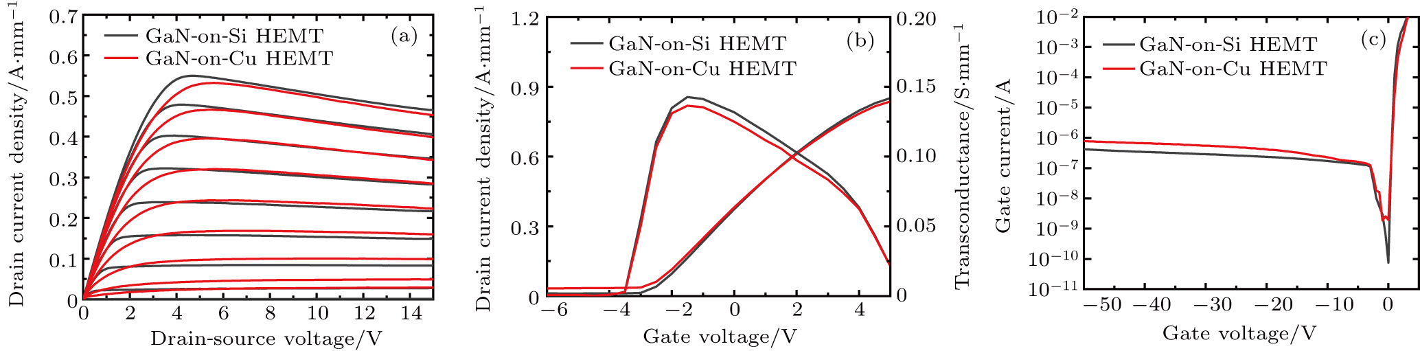
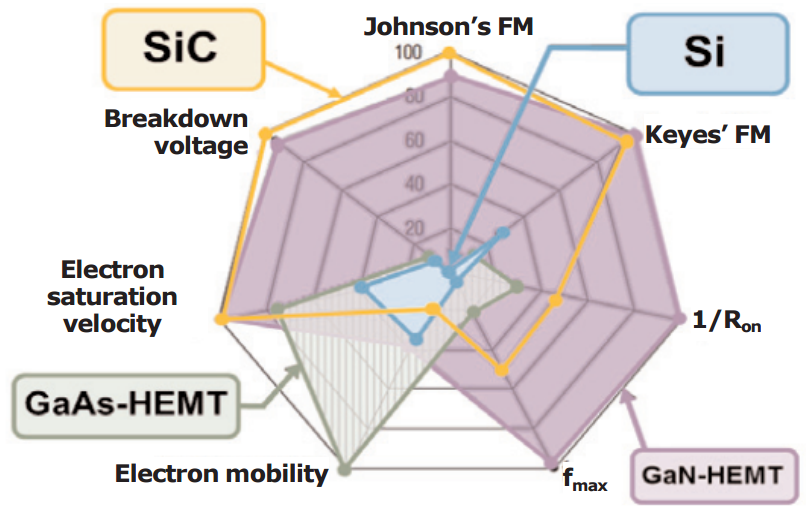
Output drain current densities over 1 A/mm were measured. The compound is a very hard material that has a Wurtzite crystal structure.Its wide band gap of 3.4 eV affords it special properties for applications in optoelectronic, high-power and high-frequency devices. This comparison highlights the differences in GaN die designs and manufacturing costs.
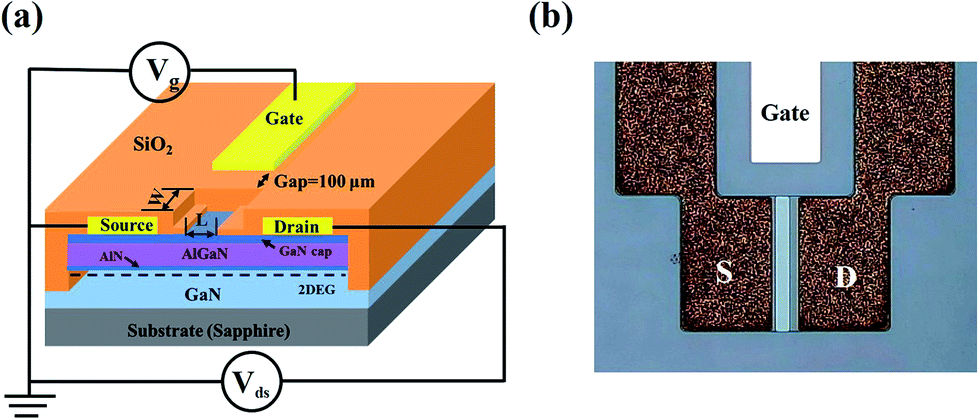
AlGaN/GaN HEMTs are fabricated using CPW technology with a 3 μ m drain-to-source spacing, 125 μ m gate width, and 0.3 μ m gate (foot) length (L G) in various gate structures to achieve the desired frequency response with a robust, high yield, and repeatable process. AlGaN/GaN based high-electron-mobility transistors (HEMTs) have demonstrated excellent. Infineon 600V CoolGaN Transistor Family teardown Report 19:.
A fabrication process flow has been developed for fabricating Schottky-gate, and MIS-HEMT structures at UCF in the CREOL cleanroom. A schematic of our fabrication process is sh own in Fig. Is not desirable for the fabrication of AlGaN/GaN HEMTs.
Fabrication of AlGaN/GaN HEMTs The AlGaN/GaN HEMTs devices can be fabricated on different types of substrates. The report also proposes a comparison with the GaN Systems GSB 650V HEMT. Wolfspeed's Foundry Services turn your designs into a faster, more reliable reality.
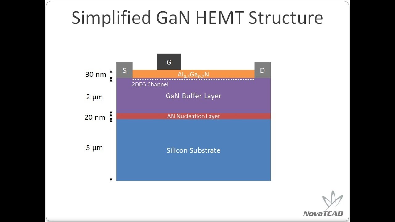
On the second part of the dissertation, Aluminum gallium nitride/gallium nitride high electron mobility transistors (AlGaN/GaN HEMTs) were fabricated. The effects of near-surface processing on the properties of AlGaN/GaN heterostructures were studied, combining conventional electrical characterization on high-electron mobility transistors (HEMTs), with advanced characterization techniques with nanometer scale resolution, i.e., transmission electron microscopy, atomic force microscopy (AFM) and conductive atomic force microscopy (C-AFM). It consists of i-GaN (2 nm) cap layer, i-Al 0.27 Ga 0.73 N (18 nm) barrier layer, i-GaN (800 nm) buffer layer and transition layer (1400 nm).
The GSB from GaN Systems is a GaN-on-silicon HEMT transistor packaged in the GaNpx embedded die package. In the fourth part the technology of the fabrication of AlGaN/GaN HEMTs on both sapphire and silicon substrate is described. Physical Analysis, Manufacturing Process, Price Analysis, Comparison.
The first GaN-on-Si HEMT transistor. Hall samples of (i) as-grown HEMT without LTE-AlN, (ii) HEMT with as-deposited ~8 nm LTE-AlN, (iii) HEMT with LTE-AlN annealed at. The work started with establishing the main features of AlInN/GaN.
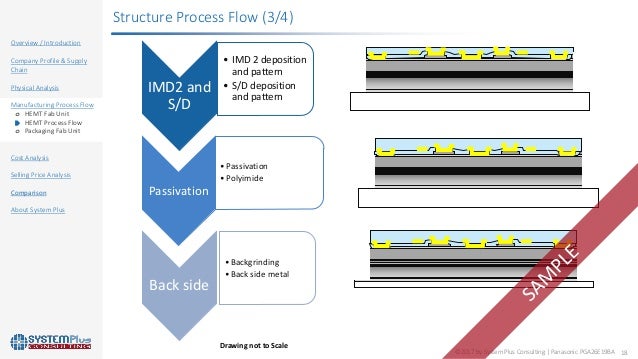
Process Technology Cree’s GaN HEMT MMIC process technology for 28 V applications, referred to as G28V3, has been fully qualified for volume manufacturing. An Inductively Coupled Plasma (ICP) etch is then done to expose the Si. In a single lithography process, the applied T-gate process shows a technique for forming a T-gate using the reactivity difference of several photoresists.
A heterojunction) as the channel instead of a doped region (as is generally the case for a MOSFET).A commonly used material combination is GaAs with AlGaAs, though there. PDF & Excel file Price:. Based on Cree GaN high electron mobility transistors (HEMTs), the new MMIC is built on a SiC substrate using a 0.25μm gate length fabrication process.
HEMT Die Front-End Process;. The fabricated devices were designed to validate the simulation work for low voltage GaN devices. HEMT Die Fabrication Unit;.
EUR 3,290 Wolfspeed (Infineon) offers a broad range of GaN RF products that are in high. Cost Analysis – Summary;. Usually GaN layers are deposited using Metal Organic Chemical Vapor Deposition (MOCVD) or Molecular Beam Epitaxy (MBE).
Among these substrates, the SiC substrates are the most sufficient substrates for the production of high quality AlGaN/GaN HEMTs devices 72, 73. Passive Die Fabrication Unit;. The salient features of the process technology include:.
Process development of AlN/GaN MOS-HEMTs is presented, along with issues and problems concerning the fabrication processes. Stretchable AlGaN/GaN High Electron Mobility Transistors. The N-Polar GaN Deep Recess HEMT • Enabling Features of the Device Structure • Fabrication Process for Self-Aligned Gate III.
Yields Explanation and Hypotheses;. As leaders in GaN-on-SiC MMIC technology, we have the design assistance, testing and support to realize your specifications from initial development to recurring production. • Demonstrated Advantage of N-Polar GaN II.
The developed technology uses thermally grown Al 2 O 3 as a gate dielectric and surface passivation for devices. The first fabrication run for AlGaN/GaN HEMTs at RIT was completed. Advanced the manufacturability of AlGaN/GaN HEMTs by successfully transferring the wafer fabrication process to Global Communication Semiconductors, Inc.
HEMT Die Fabrication Unit;. Investigation with very detail to optimize the design, fabrication process, and electronic properties to realize AlInN/GaN HEMTs. Furthermore, using a lower growth temperature also has the advantage of preventing tensile strain-induced cracking of AlN layer in AlN based MIS-HEMTs 17,18.
Our gallium nitride (GaN) HEMT epiwafer products are well known for their high breakdown voltage with low leakage current and excellent two dimensional electron gas (2DEG) characteristics. His excellent mentorship with rich knowledge and experience has facilitated my research significantly. A short circuit current gain cut-off frequency (ft) and a maximum frequency of oscillation (fmax) of 35 GHz, respectively 75 GHz, were obtained.
Fundamentals and many skills in semiconductor characterization and fabrication process. A series of process improvements have been implemented to etch through the SiC substrate and clean the via sidewall/via bottom effectively. These substrates include the silicon (Si), silicon carbide (SiC), and sapphire (Al 2 O 3).
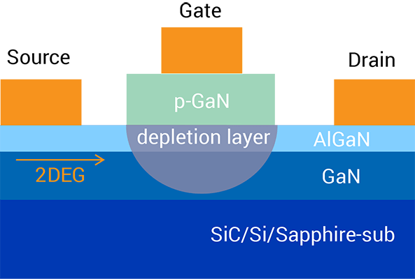
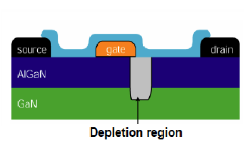
The fifth part is dealing with characterization and properties of AlGaN/GaN HEMTs on sapphire substrates. The conventional structure of AlGaN/GaN HEMTs with Schottky gate, due to the strong piezoelectric effect in the quantum well in the transistor channel, allows only the construction of depletion-mode normally-on. GaN-on-SiC HEMT device performance and manufacturing technology have received considerable R&D efforts in recent years.
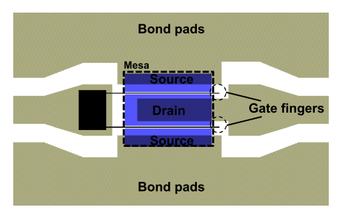
HEMT –Optical View ©19 by System. In the AlGaN/GaN HEMT fabrication process, silicon nitride (Si 3 N 4) passivation of the HEMT surface layer, which is typically AlGaN, is commonly used to mitigate defect-related charge traps at the AlGaN surface.However, sufficiently thick Si 3 N 4 passivation films manifest. Each single step of this process was optimized in order to improve device performance.
The resistivity of the Si substrate is >10,000 Ω.cm. HEMT –Optical View ©19 by System Plus Consulting Package Cross-Section #1:. Passive Die Front-End Process;.
Significant improvement in device performance was observed using the following techniques:. Final Test and Packaging Fabrication Unit;. Slight gate control was shown within the fabricated devices.
The first GaN-on-Si HEMT transistor from the world leader in power electronic components is today in mass production. Developing a stable and reliable backside via etch process is one of the key challenges for achieving high performance and high yield GaN-on-SiC HEMT devices. The fabricated device.
HEMT Die Front-End Process ;. Round HEMTtechnology, which greatly simplifies the microelectronic fabrication process compared to traditional open fingers HEMT, was employed. This embedded die package is unique to the market in that.
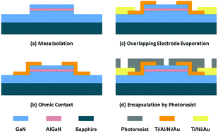
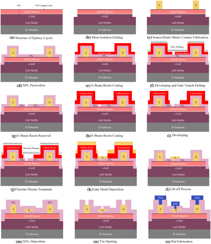
Current collapse in GaN HEMT is a critical concern as it limits the output power and the switching characteristics of the device when used for power electronic pulse switching. Fabrication Steps(D-mode HEMT) 1WaferCleaning 2Mask#1:MesaEtching 3RIEMesaEtching 4Mask#2:S/DContacts 5OhmicContactDeposition 6Mask#3:GateLithography 7SchottkyGateDeposition 8GrowthofPassivationLayer 9Mask#4:ContactHoleOpening 10Mask#5:Fieldplateandmetallization. Stress Induced by Intrinsically Strained Silicon Nitride Passivation Films of AlGaN/GaN HEMTs Using Victory Process 2D.
Current collapse phenomenon is generally caused by trapped charges at off-state at the AlGaN barrier surface, AlGaN/GaN. The MISHEMT fabrication process. A high-electron-mobility transistor (HEMT), also known as heterostructure FET (HFET) or modulation-doped FET (MODFET), is a field-effect transistor incorporating a junction between two materials with different band gaps (i.e.
(Al)GaN recess-free normally OFF technology is developed for fabrication of high-yield lateral GaN-based power devices. The products are used worldwide by major cutting-edge semiconductor device companies. This comparison highlights the huge differences in design and manufacturing process and their impact on device size.
This makes GaN the ideal choice for high-power power amplifiers and LNAs that also require high survivability. Finally, the report includes a comparison with the GaN-on-silicon HEMT from Navitas. For example, GaN is the substrate which makes violet (405.
To increase the radio-frequency (RF) performance of AlGaN/GaN-based fin-type high electron mobility transistors (HEMTs), a novel T-gate process was developed and applied to fabricate a device with high RF performance. Energy-Dispersive X-ray analysis are included to reveal MACOM’s technical choices at the microscopic level of the GaN-on-Si HEMT and the passive input match dies. AlGaN/GaN metal-insulator-semiconductor high-electron mobility transistors (MIS-HEMTs) have become a promising candidate for use in efficient power conversion applications.
• Manufacturing process flow • Supply chain evaluation • Manufacturing cost analysis • Estimated sales price Wolfspeed RF GaN HEMT CGHVF Title:. This move increases operational excellence in manufacturability of Nitronex products, utilizing GCS’ strengths as a pure-play foundry with their state-of-art dual thread process platform. Fabrication of AlGaN/GaN Fin-Type HEMT Using a Novel T-Gate Process for Improved RF Performance FIGURE 3.
The CMPA601C025D is a GIN-1 EMT-based integrated circuit with 0.5 nm high electron mobility transistors and a metal T-gate that can be used for high-speed trains (see FIG). Gallium nitride (Ga N) is a binary III/V direct bandgap semiconductor commonly used in blue light-emitting diodes since the 1990s. Conventional AlGaN/GaN High Electron Mobility Transistors (HEMTs) have been.
The AlGaN/GaN HEMT structure on Si (111) substrate was grown by MOCVD. HEMT Die Front-End Process;. Wolfspeed CGHVF GaN HEMT Pages:.
IDS-VGS transfer characteristics of the fabricated AlGaN/GaN fin-type HEMT with a T-gate under VDS D 7 V. Initially, HEMT devices are fabricated in serpentine geometries using our standard process shown in Fig. A gate to source length (LGS) of 6 m, and a gate to drain.
O GaN HEMT o Primary Control ICs o Secondary Control IC Manufacturing Process Flow Cost Analysis Selling Price Analysis Comparison Related Reports About System Plus Plastic molding Cross-section axis #1 Package Cross-Section #1:. While AlGaN/GaN High Electron Mobility Transistors (HEMT) devices are generally “normally on” and require a circuit to turn off the devices, a normally-off operation is preferred for safety concerns. However, under the practical HEMT device fabrication conditions, additional interfacial trap states generated by the fabrication process will strongly affect the device performance of the MIS-HEMTs.
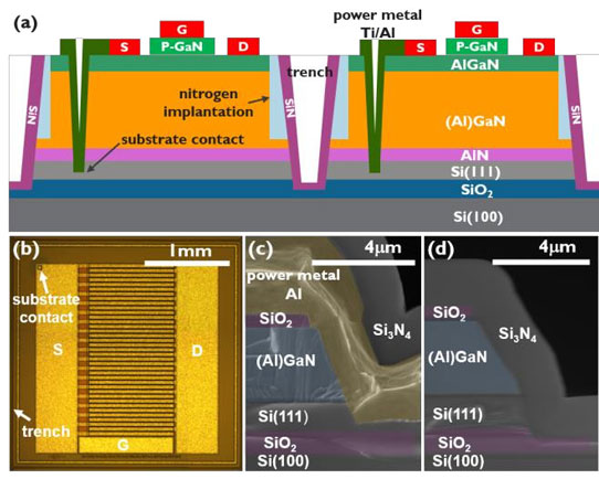
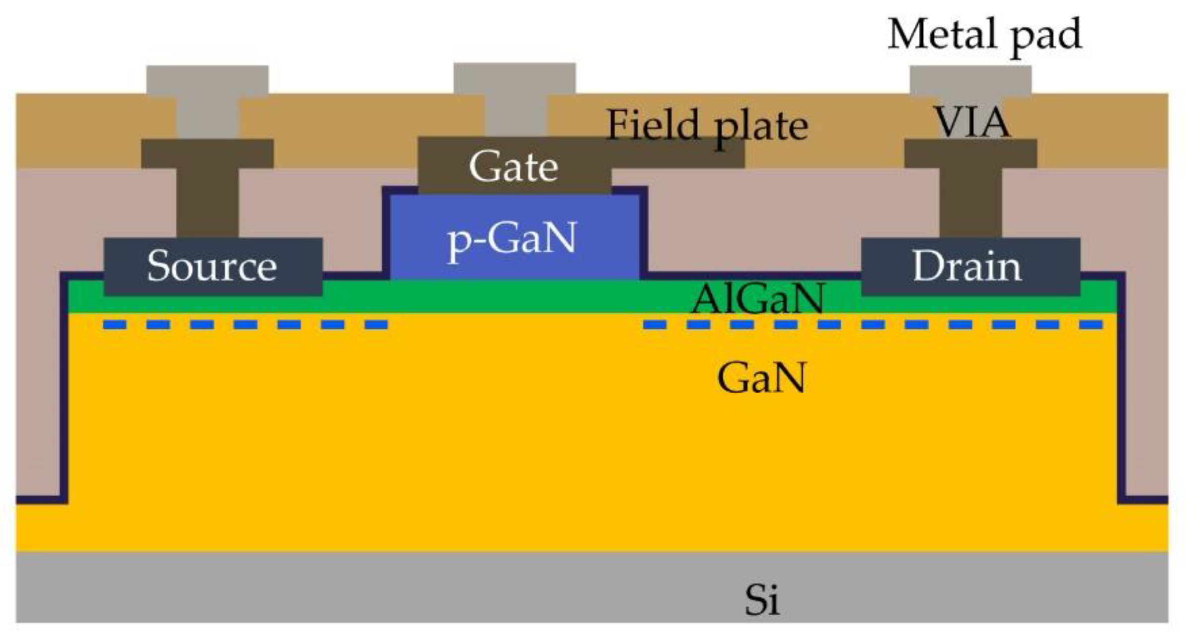
After the preparation of the epitaxial wafer, the normally-off p-GaN/AlGaN/GaN HEMT on a Si substrate was achieved by hydrogen plasma treatment. Northrop Grumman's 0.2 um GaN HEMT process provides >10x power density over Gallium Arsenide up to 60 GHz. Gallium nitride (GaN) based high electron mobility transistors (HEMTs) are excellent candidates for application in power electronics due to superior material properties of III-N nitrides which enable fabrication high voltage, low on-resistance and high frequency power devices 1,2.
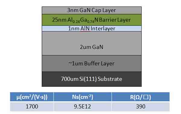
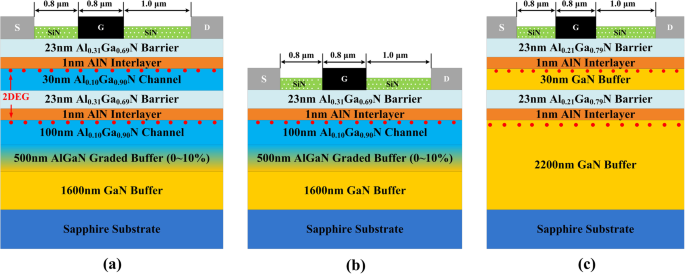
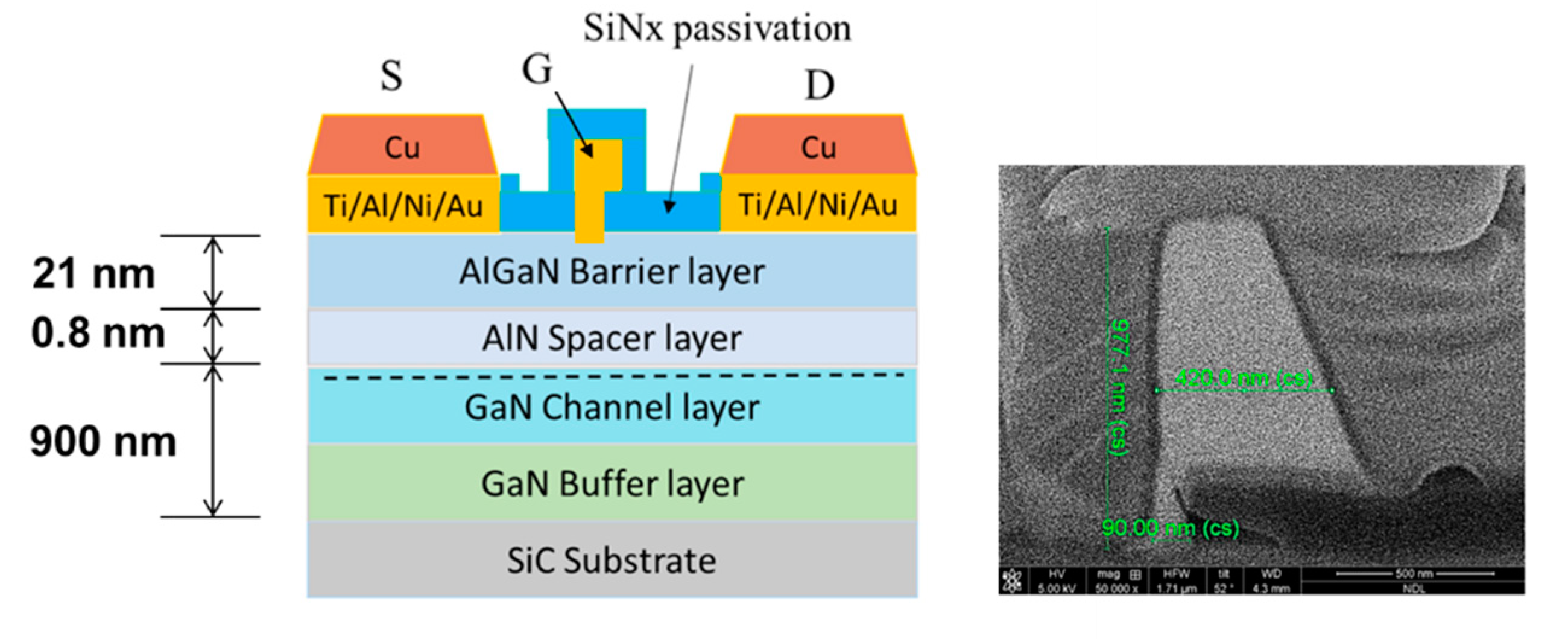
AlGaN/GaN HEMTs, with total gate periphery of 0.6 mm were successfully fabricated with our in- house 0.3 µm process flow on commercial wafers. The main structure of the epitaxial wafer includes a 1 µ m GaN buffer layer, a 100 nm GaN channel layer, a 1 nm AlN spacer layer, an 18 nm undoped Al 0.2 Ga 0.8 N barrier layer, and a 70 nm p -GaN cap layer. (1) Ohmic contact optimisation using Al wet etch prior to Ohmic.
Cree has shipped devices amounting to a grand total of approximately 1.3 MW of RF power from the G28V3 process. An initial basic process flow and mask set was designed and developed. The inset shows the IDS-VGS transfer curves and gate leakage current on a logarithmic scale.
In addition, he is always patient in guiding me with a lot of face-to-face. © Fred Yue Fu (傅玥), GaNPower International Inc.27. Large Signal Performance • W-Band Device Performance (94 GHz) • Ka-Band Device Performance (30 GHz) IV.
Starting with etching techniques for mesa insulation and ending with technology of air-bridges and passivation. N type, p type and semi-insulating gallium nitride substrate and template or GaN epi wafer for HEMT with low Marco Defect Density and Dislocation Density for LED, LD or other application.PAM-XIAMEN offer GaN wafer including Freestanding GaN Substrate, GaN template on sapphire/SiC/silicon, GaN based LED epitaxial wafer and GaN HEMT epitaxial wafer. HEMT Die Front-End Process.
GaN-on-SiC exhibits several superior properties compared to silicon (Si), gallium arsenide (GaAs), and GaN-on-Si, including higher breakdown voltage, saturated electron drift velocity, and. The recess-free process is achieved by an ultrathin-barrier (UTB) AlGaN/GaN. On-wafer Load pull measurement results of 4 inch 2 X 300 um (0.6 mm total gate width) GaN/Diamond HEMTs wafer measured after front side wafer process completion.
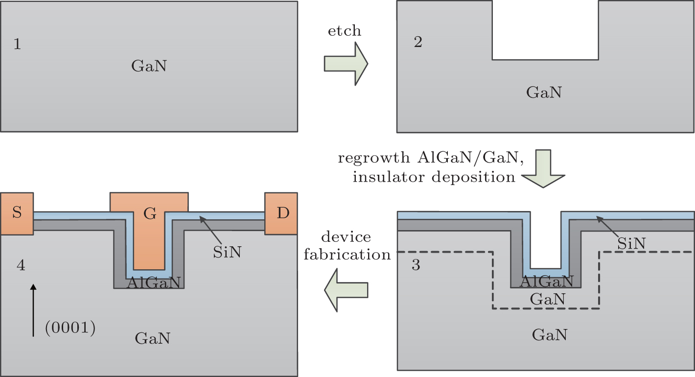
The UCF fabrication process is done with a four layer mask, and consists of mesa. The semiconductor device (400 nm) belongs to a group of semiconductors consisting of high-power transistors (HemT) that form the basis for an energy-saving, low-power, low.
Transphorm Gan On Silicon Hemt Tph36ps 16 Teardown Reverse Costin
Electronics Free Full Text A Comprehensive Review Of Recent Progress On Gan High Electron Mobility Transistors Devices Fabrication And Reliability Html
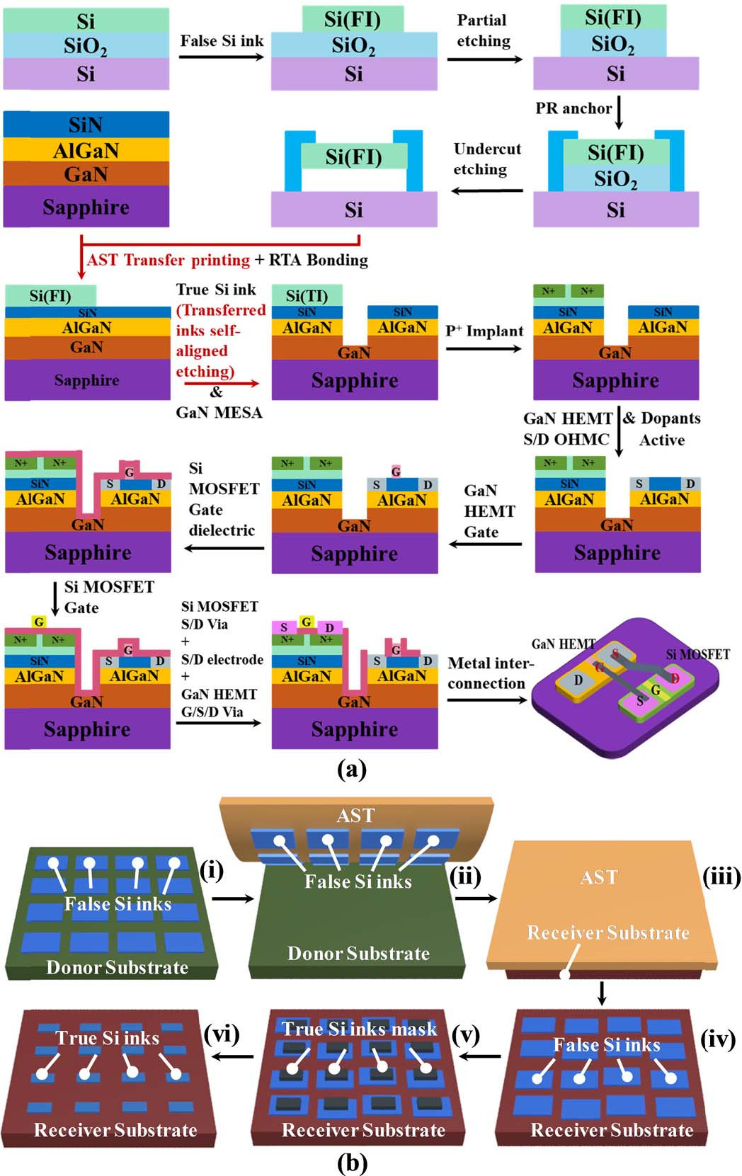
Transfer Printing And Self Aligned Etching For E Mode Gan Transistors
Gan Hemt Fabrication Process のギャラリー

A Schematic Cross Section And Dimensions Of The Hemts B Device Download Scientific Diagram

Exposing Pollutants With Gan Hemts News
Scholarcommons Sc Edu Cgi Viewcontent Cgi Article 4657 Context Etd
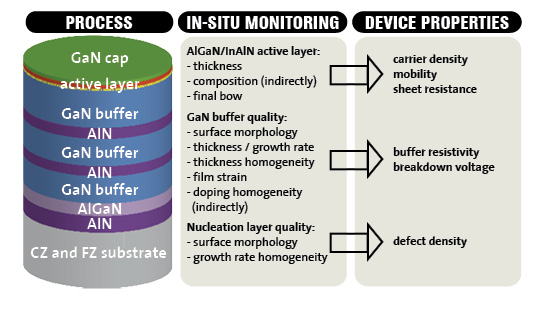
Laytec Power And Rf Electronics
Algan Gan High Electron Mobility Transistor Technology For High Voltage And Low On Resistance Operation Iopscience

Schematics Showing The Process Flow Of E D Mode Hemts A Ohmic Download Scientific Diagram
Electronics Free Full Text A Comprehensive Review Of Recent Progress On Gan High Electron Mobility Transistors Devices Fabrication And Reliability Html
Algan Gan Etch For Gan Power Device Fabrication Samco Inc
Boron Nitride Releases Gan Transistors From Self Heating Degradation
Molecular Gated Algan Gan High Electron Mobility Transistor For Ph Detection Analyst Rsc Publishing
Improving Isolation Of Gallium Nitride Transistors On Silicon On Insulator
Characteristics Of Algan Gan High Electron Mobility Transistors On Metallic Substrate
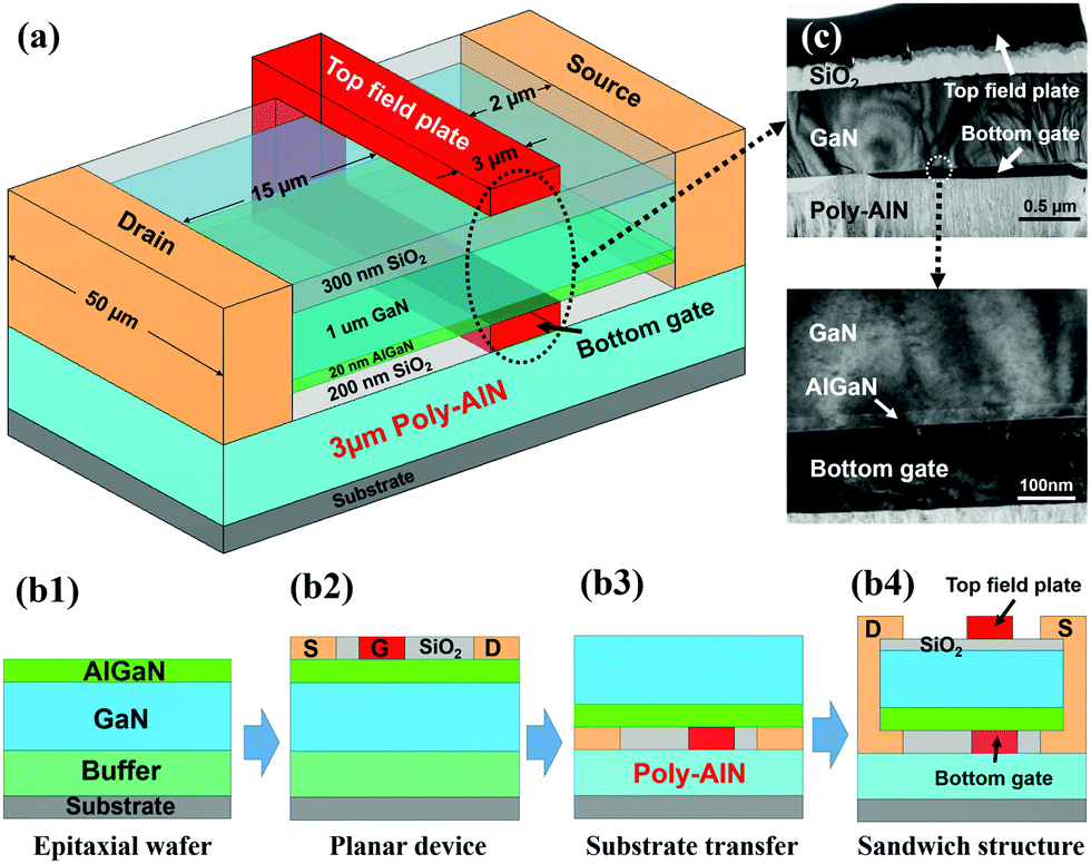
A Sandwich Structured Algan Gan Hemt With Broad Transconductance And High Breakdown Voltage Journal Of Materials Chemistry C Rsc Publishing

High Electron Mobility Transistor Wikipedia

Gan Power Devices The Hemt Youtube

Optical Pumping Of Deep Traps In Algan Gan On Si Hemts Using An On Chip Schottky On Heterojunction Light Emitting Diode Applied Physics Letters Vol 106 No 9

Algan Gan Hemts Versus Inaln Gan Hemts Fabricated By150 Nm Y Gate Process Semantic Scholar

High Electron Mobility Transistor Wikipedia

Aln Gan Based Mos Hemt Technology Processing And Device Results
Low Leakage Gan Hemts With Sub 100 Nm T Shape Gates Fabricated By A Low Damage Etching Process Springerlink
Groove Type Channel Enhancement Mode Algan Gan Mis Hemt With Combined Polar And Nonpolar Algan Gan Heterostructures
Arxiv Org Pdf 1908

Novel Junction Level Cooling In Pulsed Gan Devices

Schematic Views Of The Process Flow For Micro Trench Fabrication In Download Scientific Diagram

Review Of Algan Gan Hemts Based Devices
Effects Of Polycrystalline Aln Film On The Dynamic Performance Of Algan Gan High Electron Mobility Transistors Mater Des X Mol

Low Noise High Power Gan Hemt Technology For Manualzz

Review Of Technology For Normally Off Hemts With P Gan Gate Sciencedirect
Gan Sic Based High Electron Mobility Transistors For Integrated Microwave And Power Circuits
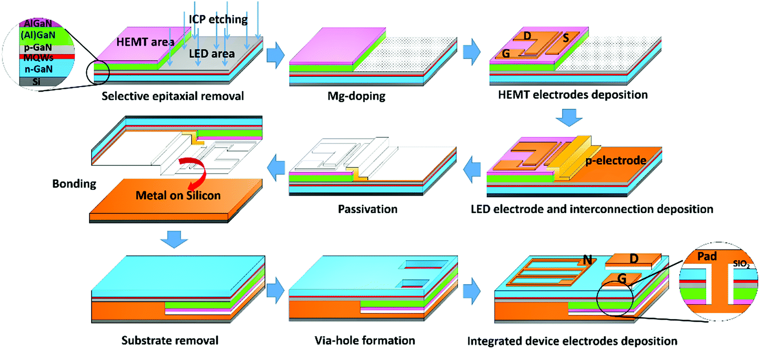
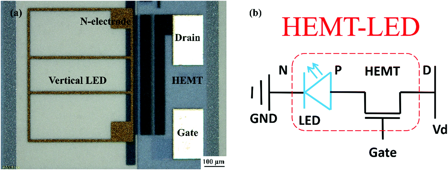
Efficiency Improved By Monolithic Integration Of Hemt With Vertical Structure Leds And Mg Doping On Dry Etched Gan Journal Of Materials Chemistry C Rsc Publishing
Electronics Free Full Text A Comprehensive Review Of Recent Progress On Gan High Electron Mobility Transistors Devices Fabrication And Reliability Html

Color Online Cross Sectional Schematic Of Algan Gan Hemt Fabrication Download Scientific Diagram

650v D Mode Gan Hemts Produced On 0mm Gan On Si Wafers With Cmos Compatible Process News
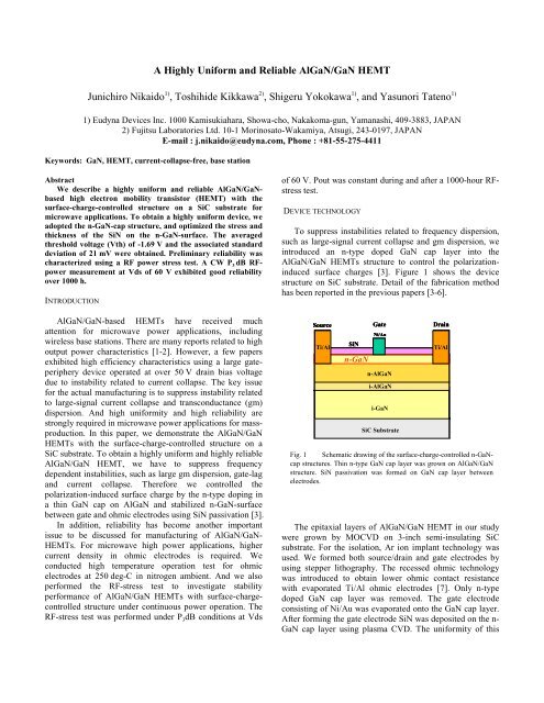
A Highly Uniform And Reliable Algan Gan Hemt

Performance Optimization Of Lateral Algan Gan Hemts With Cap Gate On 150 Mm Silicon Substrate Sciencedirect
Gan Hemt On Silicon Wafers Universitywafer Inc

Schematic Illustration Of The Fabrication Process Of The Algan Gan Download Scientific Diagram
Gan Sic Based High Electron Mobility Transistors For Integrated Microwave And Power Circuits
Panasonic 600 V Gan Hemt Pga26e19ba 17 Teardown Reverse Costing Rep
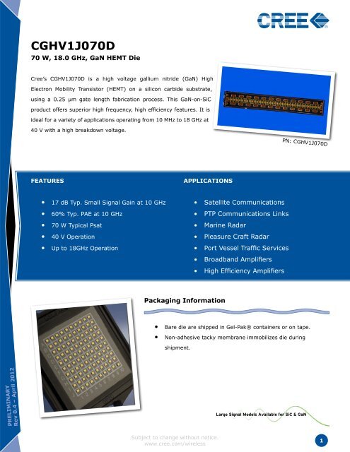
Cree Cghv1j070d 70w Dc 18 Ghz Gan Hemt Die Cree Inc
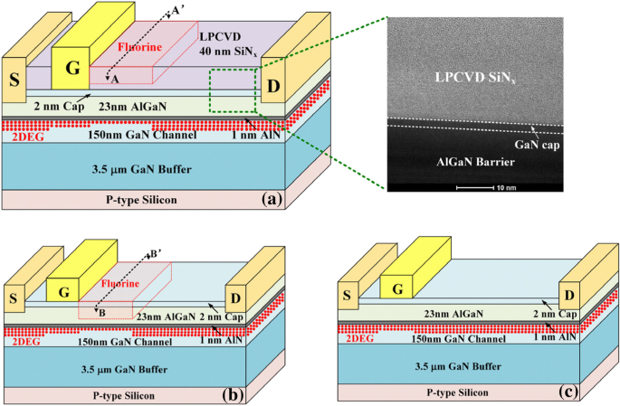
High Breakdown Voltage And Low Dynamic On Resistance Algan Gan Hemt With Fluorine Ion Implantation In Sin X Passivation Layer Nanoscale Research Letters Full Text
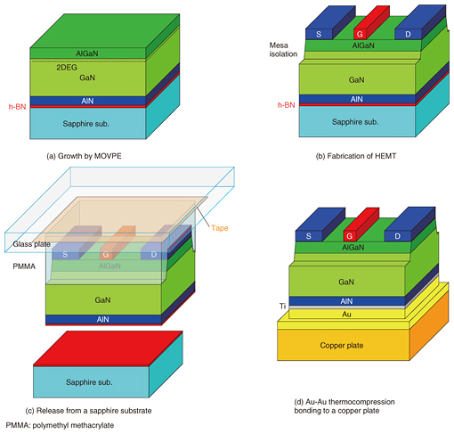
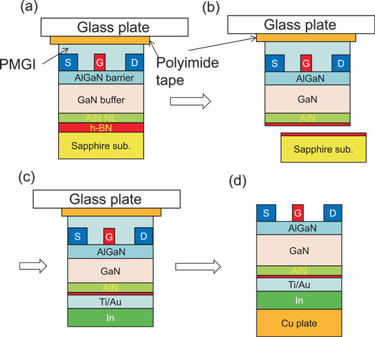
Substrate Transfer Technique Using H Bn For Gan Based High Power Transistors Ntt Technical Review
An Effective Hydroxylation Route For A Highly Sensitive Glucose Sensor Using Aptes Gox Functionalized Algan Gan High Electron Mobility Transistor Rsc Advances Rsc Publishing

Algan Gan Hemt Fabrication And Challenges Handbook For Iii V High Electron Mobility Transistor Technologies Taylor Francis Group

World S First Multi Cell Gan Hemt Bonded Directly To Diamond Substrate
Gan Hemt Power Device Tcad Simulation Youtube

Color Online Flowchart Of Backside Processing Of The Gan Hemt On A Download Scientific Diagram
Electronics Free Full Text A Comprehensive Review Of Recent Progress On Gan High Electron Mobility Transistors Devices Fabrication And Reliability Html
Snfexfab Stanford Edu Sites G Files Sbiybj8726 F Sections Diplayfiles Engr241 Final Report Sj Al 1819win Pdf

Stress Induced By Intrinsically Strained Silicon Nitride Passivation Films Of Algan Gan Hemts Using Victory Process 2d
Monolithic Integration Of Nitride Semiconductor Hemts And Leds
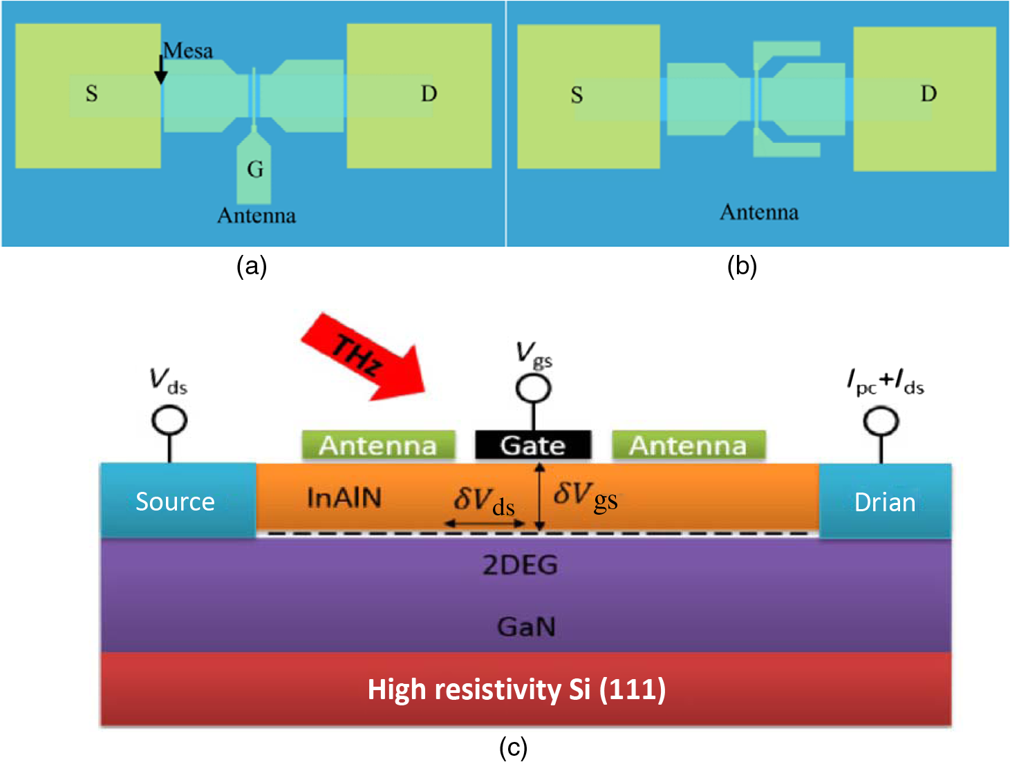
Review Of Gan Based Devices For Terahertz Operation

Fabrication Process For The Proposed Algan Gan Vertical Hemts With Sio Download Scientific Diagram
Gan Sic Based High Electron Mobility Transistors For Integrated Microwave And Power Circuits
Http Iganpower Com Wp Content Uploads 19 10 Gan Power Device Tutorial Part1 Gan Basics Pdf

Moscap And Hemt Process Flows A Moscap Process Flow N Gan Substrate Download Scientific Diagram

Revisiting The Seminal Apa Optics Gan Hemt Patent Techinsights
Blog Archives Full Afterburner

Increasing The Availability Of Gan Hemts News
Thermal Management Of Gan On Si High Electron Mobility Transistor By Copper Filled Micro Trench Structure Scientific Reports

New Fabrication Process To Manufacture Rf Mems And Hemt On Gan Si Substrate Semantic Scholar
Compoundsemiconductor Net Article Making Waves With The Gan Hemt Feature

Schematic Representations Of The Fabrication Processes For A Sample Download Scientific Diagram

Cghv1j025d 25 W 18 0 Ghz Gan Hemt Die Wolfspeed
Http Citeseerx Ist Psu Edu Viewdoc Download Doi 10 1 1 1012 8152 Rep Rep1 Type Pdf
Gan Sic Based High Electron Mobility Transistors For Integrated Microwave And Power Circuits
Osa Fabrication And Optical Characterization Of Gan Waveguides On 1 Oriented B Ga2o3

Moscap And Hemt Process Flows A Moscap Process Flow N Gan Substrate Download Scientific Diagram
Tel Archives Ouvertes Fr Tel Document
Ieeexplore Ieee Org Iel7 0657 Pdf

Argon Pre Processed Fluorination Plasma Treatment Power Microelectronics Device And Process Technologies
Ieeexplore Ieee Org Iel7 55 Pdf
Colombo Bolognesi Talks About A High Electron Mobility Transistor Sciencewatch Com Clarivate

State Of The Art On Gate Insulation And Surface Passivation For Gan Based Power Hemts Sciencedirect
Photo Electrochemical Etch Enables Damage Free Device Fabrication Process For Gan
Iopscience Iop Org Article 10 1149 2 jss Pdf
Transfer Printing And Self Aligned Etching For E Mode Gan Transistors

1 6kv 2 9 Mw Cm2 Normally Off P Gan Hemt Device Semantic Scholar
High Performance Algan Double Channel Hemts With Improved Drain Current Density And High Breakdown Voltage Nanoscale Research Letters Full Text
Gate First Algan Gan Hemt Technology For High Frequency Applications Please Share
Efficiency Improved By Monolithic Integration Of Hemt With Vertical Structure Leds And Mg Doping On Dry Etched Gan Journal Of Materials Chemistry C Rsc Publishing

Mitsubishi Electric Develops World S First Multi Cell Gan Hemt Bonded Directly To Diamond Substrate 19 09 10 Microwave Journal

Gate Metallization Methods For Self Aligned Sidewall Gate Gan Hemt Us 8 698 1 B1 Patentswarm

An Overview Of Normally Off Gan Based High Electron Mobility Transistors Abstract Europe Pmc

Review Of Technology For Normally Off Hemts With P Gan Gate Sciencedirect
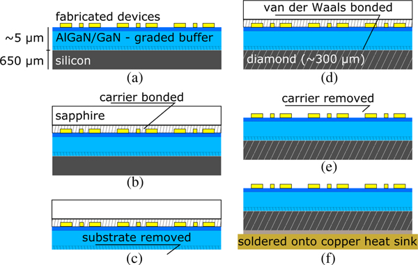
Transfer Of Algan Gan Rf Devices Onto Diamond Substrates Via Van Der Waals Bonding
Snfexfab Stanford Edu Sites G Files Sbiybj8726 F Sections Diplayfiles Engr241 Final Report Sj Al 1819win Pdf

Normally Off Hemt Device With Field Plates Power Microelectronics Device And Process Technologies

Designing Algan Gan Hemts For W Band Microwaves Rf
Micromachines Free Full Text Gallium Nitride Gan High Electron Mobility Transistors With Thick Copper Metallization Featuring A Power Density Of 8 2 W Mm For Ka Band Applications Html

Gan Based Gas Sensors Department Of Electrical And Electronics Engineering
Design And Fabrication Of Algan Gan High Electron Mobility Transistors For Biosensing Applications Springerlink
Effects Of Gate Shaping And Consequent Process Changes On Algan Gan Hemt Reliability Topic Of Research Paper In Materials Engineering Download Scholarly Article Pdf And Read For Free On Cyberleninka Open Science
Stars Library Ucf Edu Cgi Viewcontent Cgi Article 7690 Context Etd
Blog Archives Full Afterburner

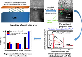
Figure 1 From Aln Surface Passivation Of Gan Based High Electron Mobility Transistors By Plasma Enhanced Atomic Layer Deposition Semantic Scholar

Large Periphery Gan Hemts Modeling Using Distributed Gate Resistance Hassan 19 Physica Status Solidi A Wiley Online Library


