Hemt Fabrication Process
HEMT Die HEMT wafer front-end cost and front-end cost per process step.

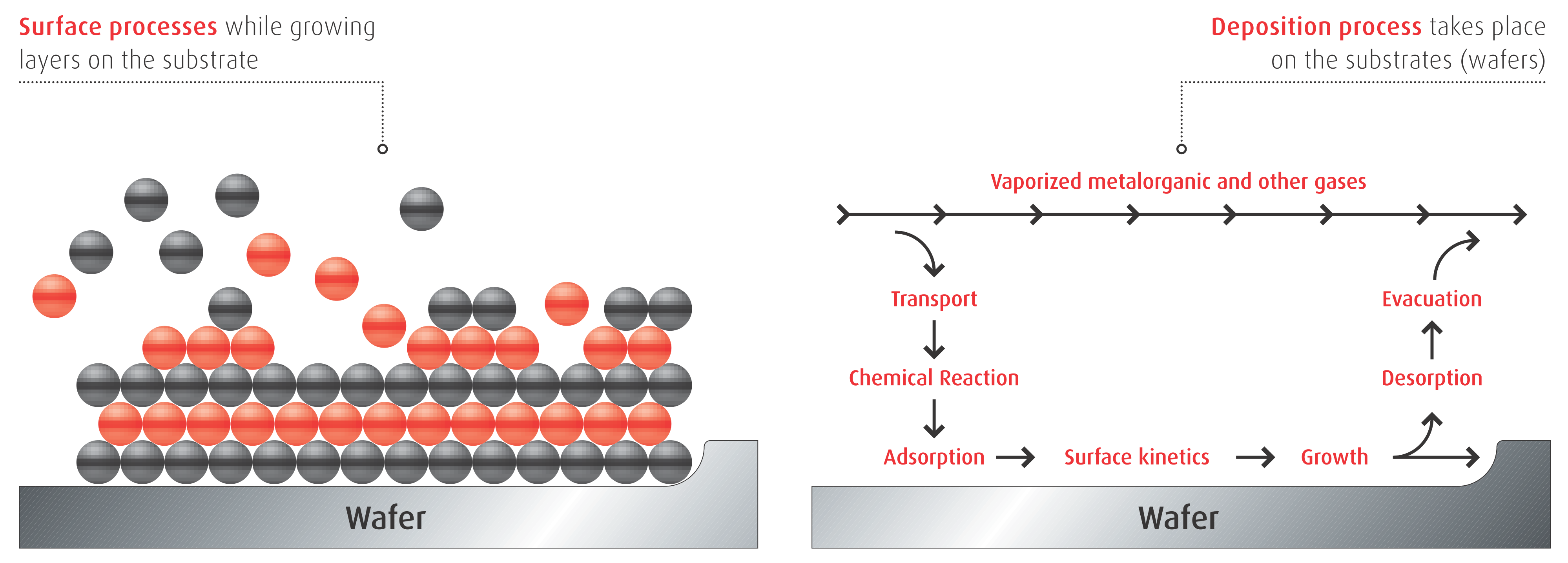
Hemt fabrication process. Currently the so-called "embedded gate process" where the gate is processed into an insulator trench is commonly used for AlGaN/GaN HEMT gate fabrication. The most common materials used aluminium gallium arsenide (AlGaAs) and gallium arsenide (GaAs). Die probe test, thinning and.
Fabrication Steps(D-mode HEMT) 1WaferCleaning 2Mask#1:MesaEtching 3RIEMesaEtching 4Mask#2:S/DContacts 5OhmicContactDeposition 6Mask#3:GateLithography 7SchottkyGateDeposition 8GrowthofPassivationLayer 9Mask#4:ContactHoleOpening 10Mask#5:Fieldplateandmetallization SimplifiedGaN-on-SapphireHEMTProcessFlow(GaN-on-siliconissimilar):. This is only about 1micron thick. Dry etch ÆInP etch stop layer removal:.
Gallium Arsenide (GaAs) HEMT Matches Technologies & Applications Northrop Grumman offers a range of GaAs pHEMT processes for matching technologies with applications. This video is a TCAD simulation tutorial for power GaN HEMT (High Electron Mobility Transistor). Manufacturing Process Flow o HEMT Fab Unit o HEMT Process Flow o ICs Fab Unit o ICs Process Flow o Component Packaging Cost Analysis Selling Price Analysis Comparison Related Reports About System Plus Description of the Wafer Fabrication Unit –IC Die 1 oIn our calculation, we simulate a production unit using 150mm wafers.
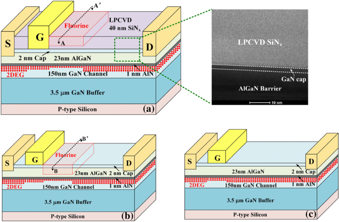
Exchange program supported by the Erasmus+ agreement between the University of Napoli federico II a. Chemical vapor deposition (PECVD) just before the HEMT fabrication process because the N-polar GaN surface is easily etched with the alkaline developer in the photolithography process.19) The gate was 10µm long. Giorgia Longobardi (Cambridge - UK).
140nm GaN 0.42m Al0.10Ga0.90N 70 nm Grad up to Al0.10 Ganm 70 AlN (HT) 0.90N. GaN-on-SiC exhibits several superior properties compared to silicon (Si), gallium arsenide (GaAs), and GaN-on-Si, including higher breakdown voltage, saturated electron drift velocity, and. FABRICATION, MODELING AND CHARACTERIZATION OF GaN HEMTs, AND DESIGN.
MBE • Molecular Beam EpitaxyMolecular Beam Epitaxy. HEMT structure & fabrication. Yield Explanations and Hypotheses;.
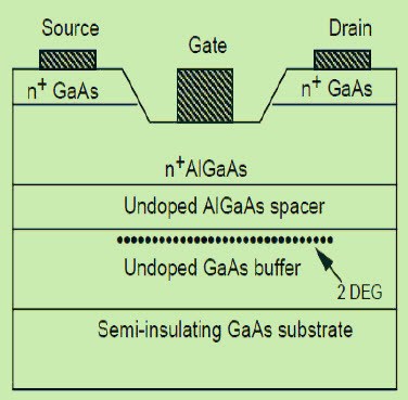
C Fabrication Process of AlGaN/GaN HEMT 101 D De-embedding 105 Bibliography 113 Acknowledgement 121 iv. Thus, an alternative approach is required in order to obtain improvement in the gate leakage. It is known as a hetero-junction and consists of a junction that uses different materials either side of the junction.
Passive Die Front-End Process;. Gallium Nitride (GaN) HEMTs (High Electron Mobility Transistors) are the next generation of RF power transistor technology.Thanks to GaN technology,PAM-XIAMEN now offer AlGaN/GaN HEMT Epi Wafer on sapphire or Silicon,and AlGaN/GaN on sapphire template. Foundry and material analysis services NTT-AT also provides process services (including MEMS device prototyping, and etching services) and material analysis services.
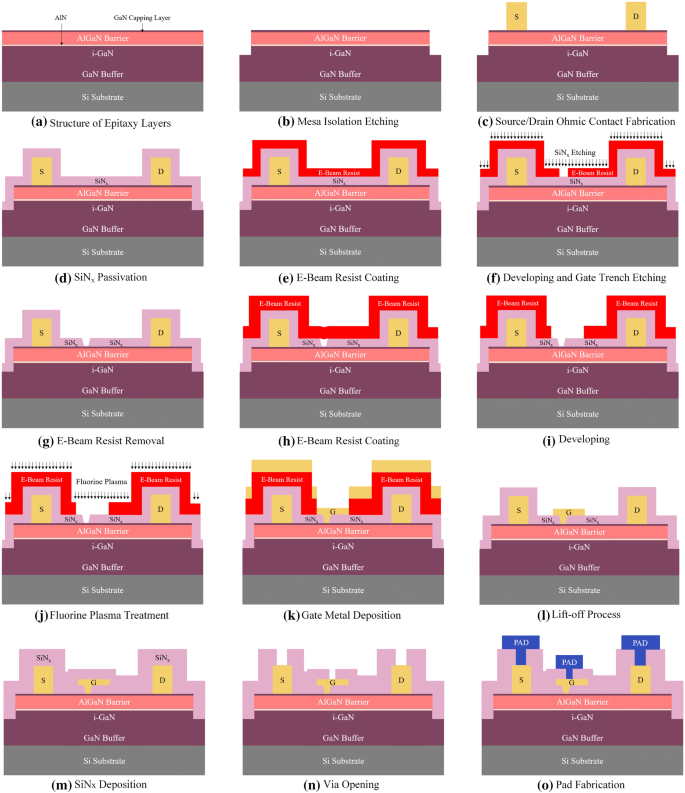
The key element within a HEMT is the specialised PN junction that it uses. The work started with establishing the main features of AlInN/GaN heterostructure in a HEMT configuration through optimizing the device fabrication and investigation of the DC characteristics of planar HEMTs. The process modules for the GaN HEMT device fabrication include device isolation, p-GaN gate formation, contacts for source and drain, contact for gate, surface passivation and so forth.
Welcome to APEX Plastics - Blow Molding Manufacturing Experts. GaAs pHEMT technology is suitable for cellular backhaul, linear digital radios, V-band, E-band and W-band radar applications, among others. In order to verify the compatibility of the process with device fabrication, electron mobility and sheet density were measured using Van der Pauw structures at room temperature on a metamorphic InGaAs/InAlAs HEMT structure before and after deposition and etching of a 300 nm silicon nitride film.
Each single step of this process was optimized in order to improve device performance. After that, a very thin layer between 30 and 60 Angstroms of intrinsic Aluminium Gallium Arsenide is set down on top of this layer. In general, a Cl 2 based mixture gas is used to etch GaN.15,16) In addition, to reduce damage from the etching, the inductively coupled plasma reactive ion etching (ICP-RIE) technique is com-monly applied.17) For electrical isolation of the HEMT fabrication process in this study, ICP dry etching with.
In this thesis, a comprehensive study of normally-off high-electron-mobility transistors is presented, including theoretical background review, theoretical analysis, physically-based device simulations, device fabrication and optimization and. We introduced two-stage balanced PA. We have expertise in fabrication of various types of structural works, water tanks, fixed type water tanks, diesel tank, frack tanks, etc.
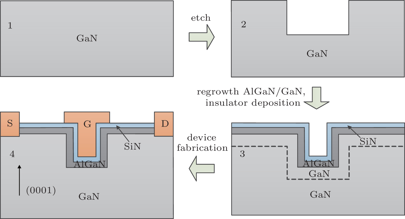
A III-nitride semiconductor layer having an active region;. While AlGaN/GaN High Electron Mobility Transistors (HEMT) devices are generally “normally on” and require a circuit to turn off the devices, a normally-off operation is preferred for safety concerns. The gate-first fabrication process flow began with plasma.
We can also provide device manufacturing and material analysis. Alcatel Speeder 100 SiO 2. Structure to be used.
A voltage source coupled to the pair of Schottky metal conductive contacts to generate an electric field sufficiently high to alter. GaN Transistor Fabrication Process. The HEMT structure consisted of a nm Al 0.25Ga 0.75N barrier layer on a 150nm GaN channel/buffer.
Fabrication HEMT has a fully equipped fabrication shop, capable to carry out fabrication of various types of process equipments like pressure vessel, heat exchangers, separator, columns etc. In the 100mm InP HEMT process, fabrication of the MIM capacitor is started at the beginning of the MMIC process prior to the completion of the HEMT device using a double-layer nitride process. Passive Die Fabrication Unit;.
Wet etch Æn+InGaAs/InAlAs multi-layer cap removal • 2ndstep:. GaN Systems wants to compete with EPC, the market leader, in the low-voltage HEMT market. The whole process flow to fabricate a HEMT mainly includes five steps, namely mesa isolation, ohmic contact formation, gate formation, pad and.
Wet EtchWet Etch Selectively remove material Chemical ProcessChemical Process Chemical Bath Patterned Photo-resist Wafer in Process Lecture 2 Fabrication Processes. A backside via etch process for both circular and slot vias through the SiC substrate has been successfully developed and qualified for the fabrication of GaN-on-SiC HEMT MMIC devices. HEMT Die Fabrication Unit;.
Yield Explanations and Hypotheses;. On the second part of the dissertation, Aluminum gallium nitride/gallium nitride high electron mobility transistors (AlGaN/GaN HEMTs) were fabricated. IC Die Front-End Processes and Fabrication Units;.
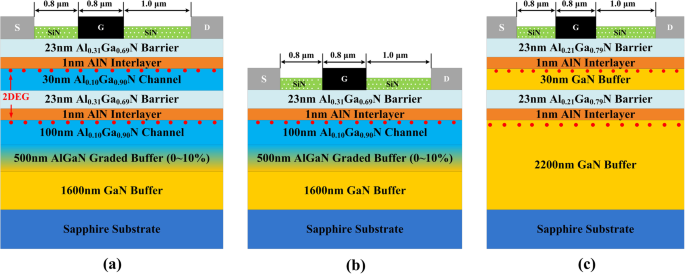
12 nm Al0.30Ga0.70N 10 nm Al2 Ga0.70 N:Si nm Al0.30 Ga0.70N 0.30 1 nm AlN. Properties to realize AlInN/GaN HEMTs. In this paper, we systematically investigate the effect of hydrogen plasma treatment radio frequency (RF) power, treatment time, and rapid thermal annealing (RTA) on the performance of high-resistivity-cap-layer high-electron-mobility-transistor (HRCL-HEMT).
Summary of the Cost Analysis;. IC Die Front-End Processes and Fabrication Units;. HEMT Die Front-End Process and Fabrication Unit;.
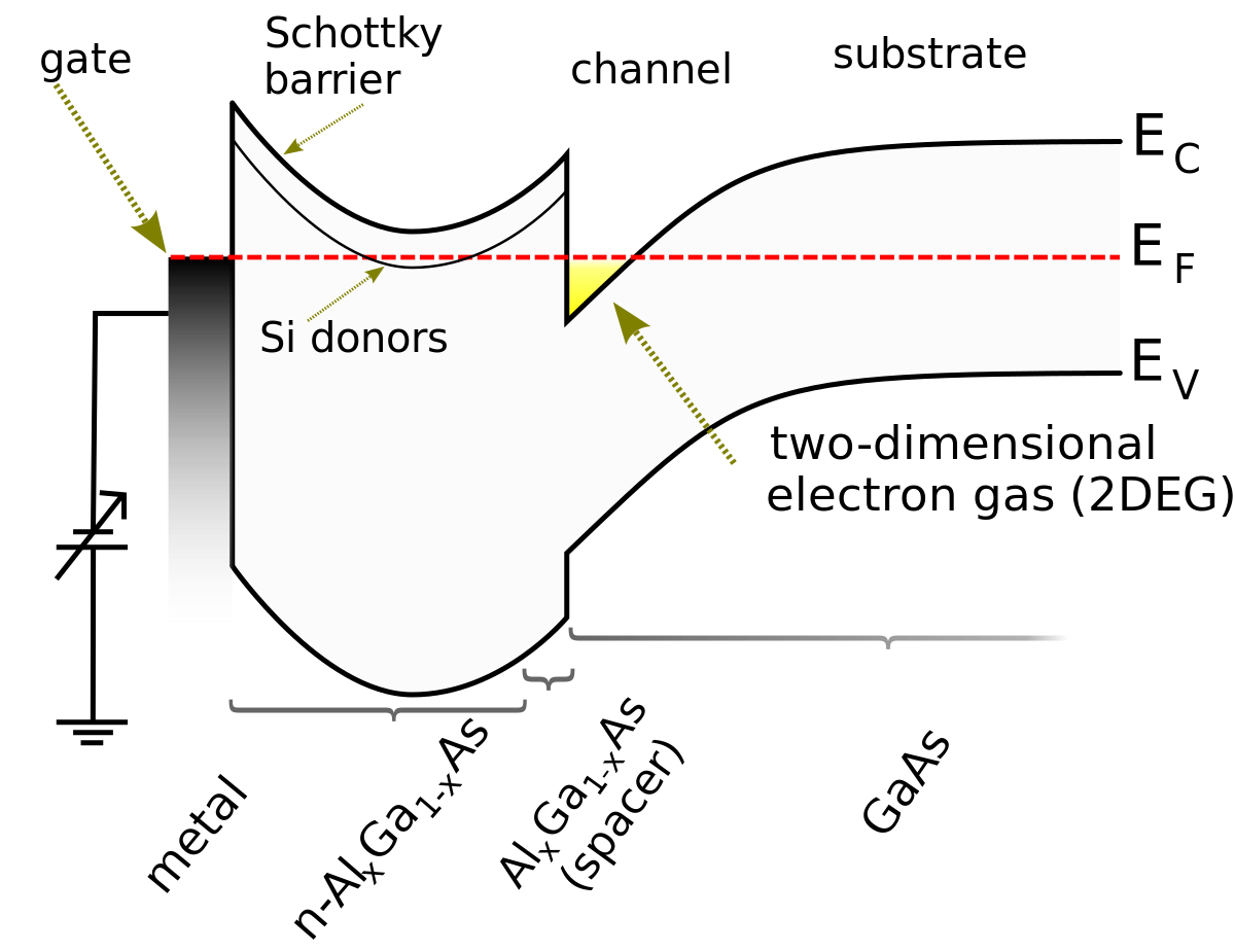
In this study, we report a fabrication process of a normally-off GaN MIS-HEMT with a gate leakage current as low as on the order of 10 −11 A/mm by exploiting a hydrofluoric (HF) acid pre-treatment prior to gate formation. What is claimed is:. A high-electron-mobility transistor, also known as heterostructure FET or modulation-doped FET, is a field-effect transistor incorporating a junction between two materials with different band gaps as the channel instead of a doped region.
Technical parameters Deosited by ICPCVD SiH4/N2/Ar=2.8/9/90sccm Power 0W Pressure 35mTorr. Initially, HEMT devices are fabricated in serpentine geometries using our standard process shown in Fig. For isolating neighbor-ing FETs, all epitaxial layers in the region between FETs were etched by Cl 2-based inductively coupled plasma.
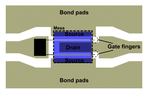
In addition, the feed pads to the gate fingers are optically printed by I-line exposure. A detailed explanation of how to edit the process input file. GAN HIGH ELECTRON MOBILITY TRANSISTORS 8 2.1 GAN MATERIAL PROPERTIES8 2.2 PRINCIPLE OF GAN HEMT S.
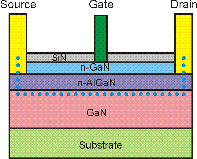
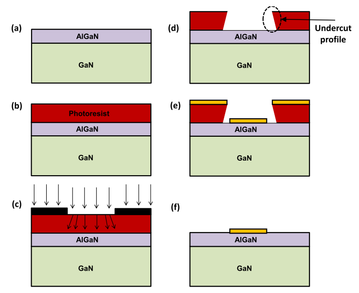
A key process in this study is dry etching. Process flow for fabrication of protected and passivated AlN/GaN MOS-HEMTs using the gate wrap-around technique. A commonly used material combination is GaAs with AlGaAs, though there is wide variation, dependent on the application of the device.
System Plus Consulting unveils the GSB from GaN Systems, the latest device driving 100V and optimized for AC-DC converters and high-frequency, high-efficiency power conversion. MESFET HEMT Oscillator –. This chapter describes a few key process steps to fabricate GaN high-electron-mobility transistors (HEMTs) for power electronics applications.
The sample is then mounted to glass slides using epoxy with. Lecture given by Dr. An optically controlled Schottky diode-based transistor comprising:.
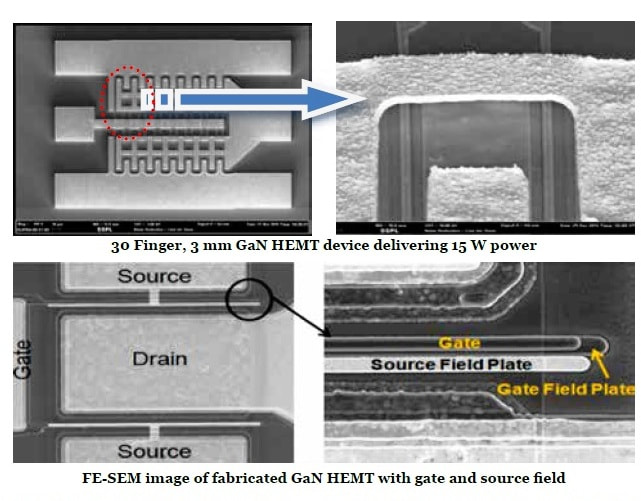
Large Signal Performance • W-Band Device Performance (94 GHz) • Ka-Band Device Performance (30 GHz) IV. Devices incorporating more indium generally show better high-frequency performance, while in recent years, gallium nitride HEMT. HEMT Wwafer front-end cost and front-end cost per process step;.
Herein, we have demonstrated highly sensitive. HEMT Die Front-End Process and Fabrication Unit;. The high electron mobility transistor (HEMT)-based biosensors are highly competitive in the ultimate application of portable and point-of-care testing.
A pair of co-planar Schottky metal conductive contacts coupled to the III-nitride semiconductor layer;. Power HEMT using field plate Submitted By :- Vivek Kumar Surana. Critical Process for Nano-HEMT Buffer Channel Insulator Cap ZEP Buffer Channel Insulator ZEP Ar-based plasma & ALET InP InP Wet etching Two-step recess for HEMT fabrication • 1ststep:.
Manufacturing Process Flow - GaN HEMT Process Flow and Fabrication Units - Resistor Process Flow and Fabrication Units - MOSFET Process Flow and Fabrication Units - Package Process Flow 6. Summary of the Cost Analysis;. GaN HEMT devices are particularly significant in power electronics applications.
IPS is a full-service solutions provider and equipment distributions firm representing a complete line of process equipment, pumps, water/waste treatment systems, mixers, heat exchangers, valves, motors and drives as well as other related. 3 SiC STEP 1 SiNx passivation 300nm SiNx. Studies on Fabrication and Reliability of GaN High-Resistivity-Cap-Layer HEMT Abstract:.
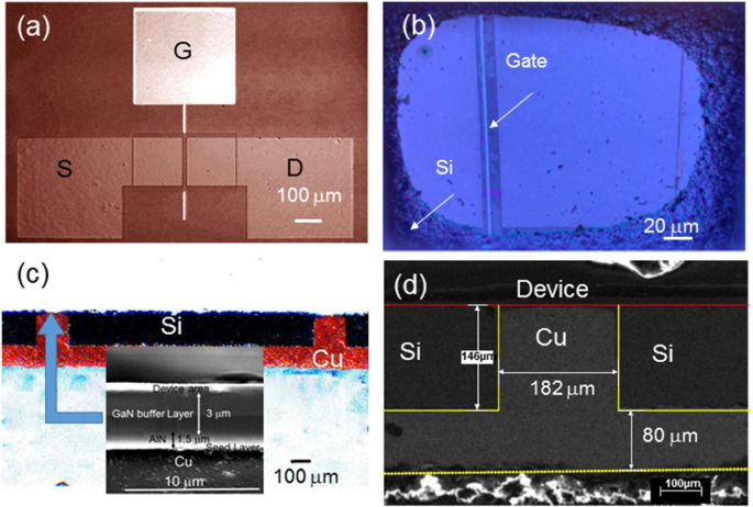
Processing includes (a) sample cleaning and deoxidation, (b) 2 nm Al deposition, (c) etching Ohmic regions and thermal oxidation of Al, (d) Ohmic metallisation and annealing, and (e) gate metallisation and device measurements. The two-dimensional electron gas (2DEG) channel was formed near the GaN/AlGaN interface with 1.0x10¹³/cm2 carrier density, 1.5x10 3cm2/V-s mobility, and 450Ω/square sheet resistance. Based on Cree GaN high electron mobility transistors (HEMTs), the new MMIC is built on a SiC substrate using a 0.25μm gate length fabrication process.
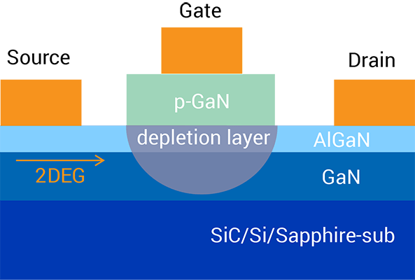
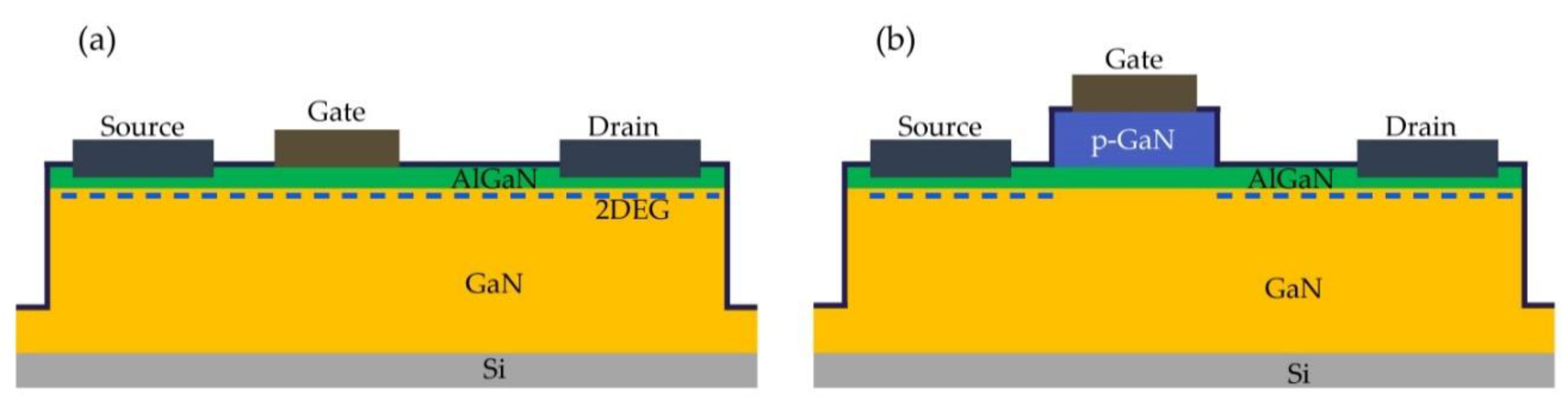
APEX Plastics is dedicated to manufacturing high quality blow-molded plastic products, providing timely deliveries and creating an atmosphere of continuous improvements where all employees strive to keep both internal and external customers satisfied. An Inductively Coupled Plasma (ICP) etch is then done to expose the Si substrate (Fig. In this section, we will focus on some of the key process technologies for the fabrication of p-GaN E-mode AlGaN/GaN HEMTs, discuss some of the challenges and.
Wafer in Process Lecture 2 Fabrication Processes. A schematic of our fabrication process is sh own in Fig. A series of process improvements have been implemented to etch through the SiC substrate and clean the via sidewall/via bottom effectively.
The N-Polar GaN Deep Recess HEMT • Enabling Features of the Device Structure • Fabrication Process for Self-Aligned Gate III. GaAs pHEMT process of UMS foundry. In a today´s world of semiconductor devices silicon transistors dominate, while GaAs-based high mobility transistors (HEMTs) and heterojunction bipolar transistors (HBTs).
In this paper, we present a method for removing a high electron mobility transistor (HEMT) silicon substrate using mechanical grinding and deep silicon etching technology and successfully transferred the epitaxial wafer to a PET substrate to achieve the flexible normally-off HEMT. HEMT Die Front-End Process;. Summary of the Cost Analysis;.
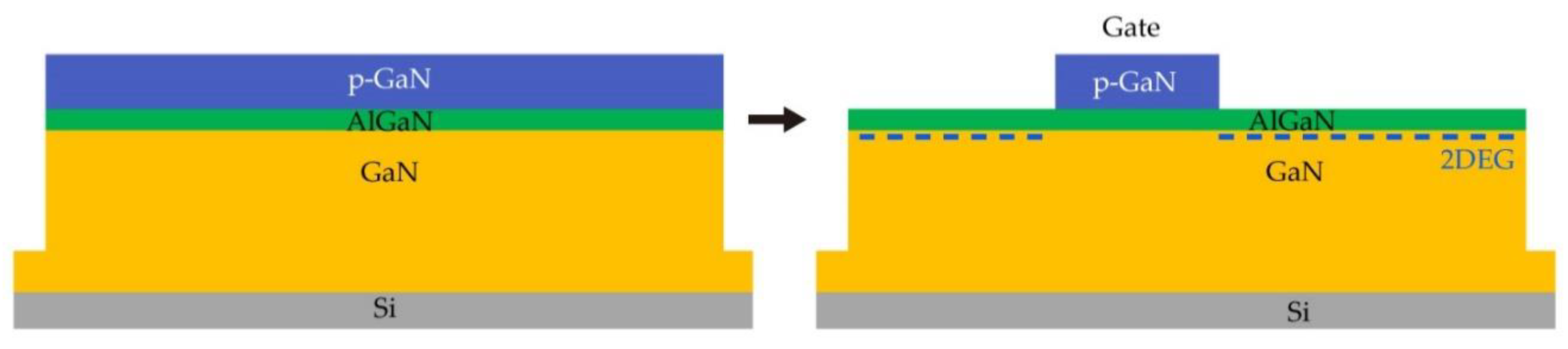
The process modules for the GaN HEMT device fabrication include device isolation, p-GaN gate formation , contacts for source and drain , contact for gate , surface passivation and so forth. The Alcatel "Speeder 100SiO 2" is an ICP Etching system which is configured for etch silicon using either the patented BOSCH Deep Silicon Etch Process or a Cryogenic etch process that are typically used in MEMS (Micro-ElectroMechanical Systems), microfluidics, and silicon masters for soft lithography stamps.The system is setup to process 4" wafers and uses etch masks. One of the challenges in GaN power device fabrication is to achieve a “normally off” operation.
CNA CN.2A CNA CNA CN A CN A CN A CN A CN A CN A CN A CN A CN A Authority CN China Prior art keywords hemt dorsal pore gaas gallium arsenide plating Prior art date Application number CN.2A. The manufacture of an HEMT as follows procedure, first an intrinsic layer of Gallium Arsenide is set down on the semi-insulating Gallium Arsenide layer.

Figure 1 From In0 17al0 n Aln Gan Triple T Shape Fin Hemts With Gm 646 Ms Mm Ion 1 03 A Mm Ioff 1 13 µa Mm Ss Mv Dec And Dibl 28 Mv V At Vd 0 5 V Semantic Scholar
Http Citeseerx Ist Psu Edu Viewdoc Download Doi 10 1 1 1012 8152 Rep Rep1 Type Pdf
High Electron Mobility Transistor Wikipedia
Hemt Fabrication Process のギャラリー

Process Flow For Fabrication Of Protected And Passivated Aln Gan Download Scientific Diagram
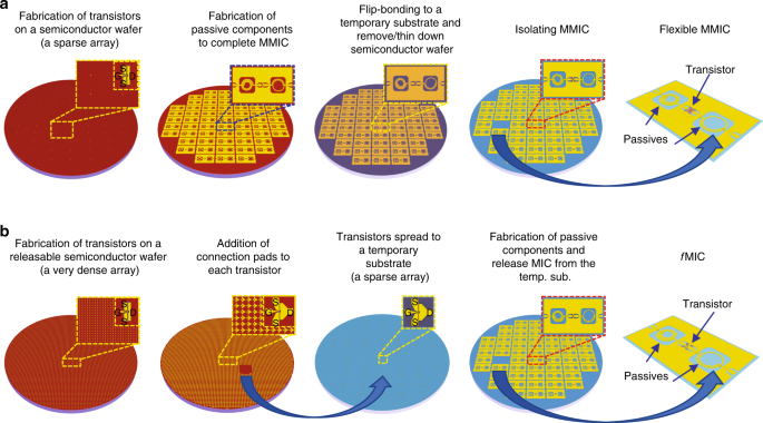
Heterogeneously Integrated Flexible Microwave Amplifiers On A Cellulose Nanofibril Substrate Nature Communications

Moscap And Hemt Process Flows A Moscap Process Flow N Gan Substrate Download Scientific Diagram

New Fabrication Process To Manufacture Rf Mems And Hemt On Gan Si Substrate Semantic Scholar
Iopscience Iop Org Article 10 1149 2 jss Pdf
Gan Sic Based High Electron Mobility Transistors For Integrated Microwave And Power Circuits

Schematic Representations Of The Fabrication Processes For A Sample Download Scientific Diagram
Stars Library Ucf Edu Cgi Viewcontent Cgi Article 7690 Context Etd
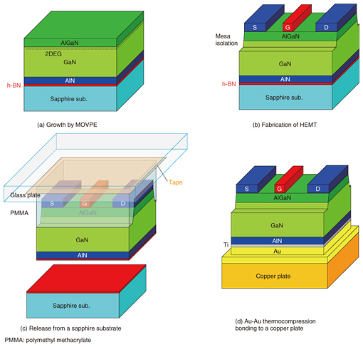
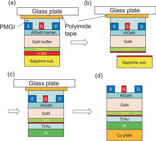
Substrate Transfer Technique Using H Bn For Gan Based High Power Transistors Ntt Technical Review
Electronics Free Full Text A Comprehensive Review Of Recent Progress On Gan High Electron Mobility Transistors Devices Fabrication And Reliability Html

Figure 3 From 1 6kv 2 9 Mw Cm2 Normally Off P Gan Hemt Device Semantic Scholar
Electronics Free Full Text A Comprehensive Review Of Recent Progress On Gan High Electron Mobility Transistors Devices Fabrication And Reliability Html

Review Of Technology For Normally Off Hemts With P Gan Gate Sciencedirect

650v D Mode Gan Hemts Produced On 0mm Gan On Si Wafers With Cmos Compatible Process News
Electronics Free Full Text A Comprehensive Review Of Recent Progress On Gan High Electron Mobility Transistors Devices Fabrication And Reliability Html

Wolfspeed Cghvgan On Silicon Hemt Chip And Module Fabrication Process Overview
Micromachines Free Full Text Novel High Energy Efficiency Algan Gan Hemt With High Gate And Multi Recessed Buffer Html
Q Tbn 3aand9gcsrmh6hxn2xcbtvnht2hdks4ohqsytrioqtpw Usqp Cau
Blog Archives Full Afterburner
Boron Nitride Releases Gan Transistors From Self Heating Degradation

Figure 1 From Aln Surface Passivation Of Gan Based High Electron Mobility Transistors By Plasma Enhanced Atomic Layer Deposition Semantic Scholar

Cree Cghv1j070d 70w Dc 18 Ghz Gan Hemt Die Cree Inc

Algan Gan Hemts Versus Inaln Gan Hemts Fabricated By150 Nm Y Gate Process Semantic Scholar
Micromachines Free Full Text Novel High Energy Efficiency Algan Gan Hemt With High Gate And Multi Recessed Buffer Html
Scholarcommons Sc Edu Cgi Viewcontent Cgi Article 4657 Context Etd

Fabrication Of 22 Nm T Gates For Hemt Applications Sciencedirect

Fabrication Process For The Proposed Algan Gan Vertical Hemts With Sio Download Scientific Diagram

Review Of Technology For Normally Off Hemts With P Gan Gate Sciencedirect

Gan Power Devices The Hemt Youtube

Schematic Illustration Of The Fabrication Process Of The Algan Gan Download Scientific Diagram
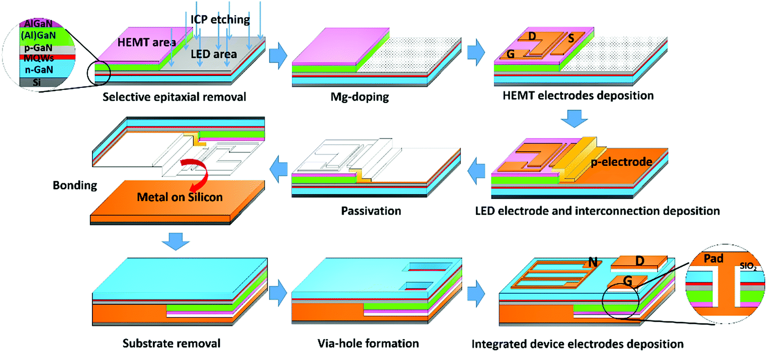
Efficiency Improved By Monolithic Integration Of Hemt With Vertical Structure Leds And Mg Doping On Dry Etched Gan Journal Of Materials Chemistry C Rsc Publishing
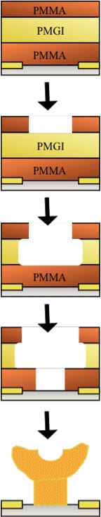
T Gate Fabrication Using Pmgi And Pmma Kayaku Advanced Materials

Small Signal Model Parameters Analysis Of Gan And Gaas Based Hemts Over Temperature For Microwave Applications Sciencedirect
Blog Archives Full Afterburner
Efficiency Improved By Monolithic Integration Of Hemt With Vertical Structure Leds And Mg Doping On Dry Etched Gan Journal Of Materials Chemistry C Rsc Publishing
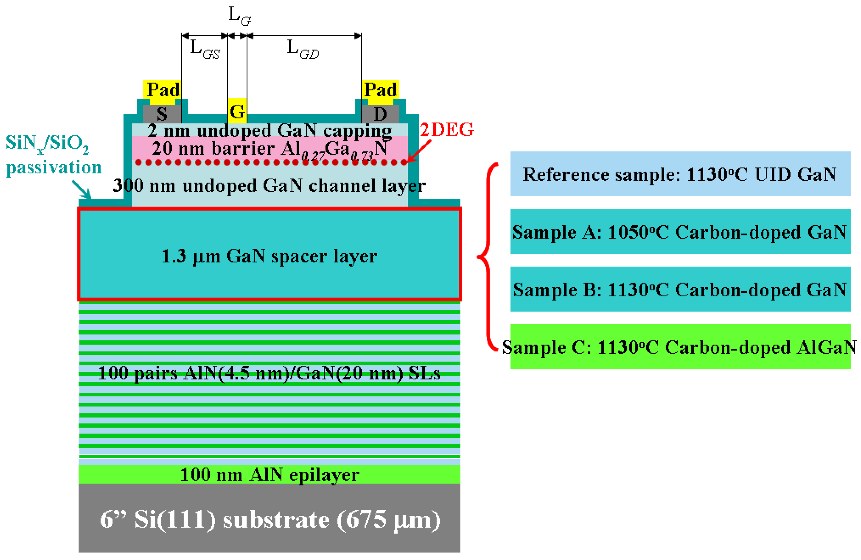
Electronics Free Full Text An Investigation Of Carbon Doping Induced Current Collapse In Gan On Si High Electron Mobility Transistors Html
Gan Sic Based High Electron Mobility Transistors For Integrated Microwave And Power Circuits

Low Noise High Power Gan Hemt Technology For Manualzz

World S First Multi Cell Gan Hemt Bonded Directly To Diamond Substrate

A Schematic Cross Section And Dimensions Of The Hemts B Device Download Scientific Diagram
Low Leakage Gan Hemts With Sub 100 Nm T Shape Gates Fabricated By A Low Damage Etching Process Springerlink
High Performance Algan Double Channel Hemts With Improved Drain Current Density And High Breakdown Voltage Nanoscale Research Letters Full Text
2

Schematics Showing The Process Flow Of The Ln Zno Algan Gan Hemts A Download Scientific Diagram

Mitsubishi Electric Develops World S First Multi Cell Gan Hemt Bonded Directly To Diamond Substrate 19 09 10 Microwave Journal
Gan Sic Based High Electron Mobility Transistors For Integrated Microwave And Power Circuits
Thermal Management Of Gan On Si High Electron Mobility Transistor By Copper Filled Micro Trench Structure Scientific Reports

Cghv1j025d 25 W 18 0 Ghz Gan Hemt Die Wolfspeed
High Electron Mobility Transistor Hemt Construction And Applications
Groove Type Channel Enhancement Mode Algan Gan Mis Hemt With Combined Polar And Nonpolar Algan Gan Heterostructures

Color Online Cross Sectional Schematic Of Algan Gan Hemt Fabrication Download Scientific Diagram
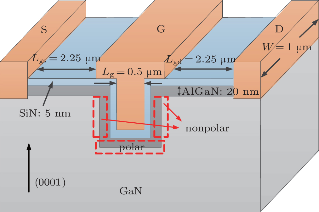
Groove Type Channel Enhancement Mode Algan Gan Mis Hemt With Combined Polar And Nonpolar Algan Gan Heterostructures

Device With Process Simplification And Ar Pretreatment Of Al2o3 Before F Plasma Treatment To Create Deeper Electron Traps For High Temperature Operation Power Microelectronics Device And Process Technologies

Algan Gan Hemt Fabrication And Challenges Handbook For Iii V High Electron Mobility Transistor Technologies Taylor Francis Group

Aln Gan Based Mos Hemt Technology Processing And Device Results
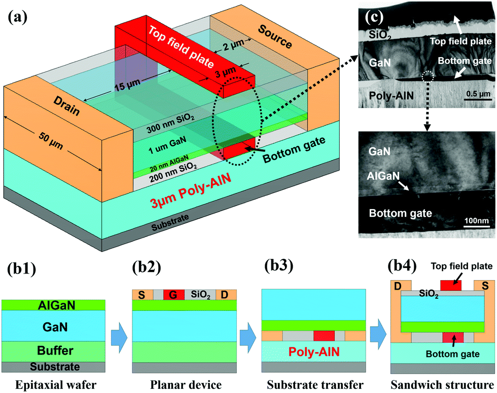
A Sandwich Structured Algan Gan Hemt With Broad Transconductance And High Breakdown Voltage Journal Of Materials Chemistry C Rsc Publishing Doi 10 1039 C9tcg
Panasonic 600 V Gan Hemt Pga26e19ba 17 Teardown Reverse Costing Rep
Gan Based Gas Sensors Department Of Electrical And Electronics Engineering
Transfer Printing And Self Aligned Etching For E Mode Gan Transistors
Electronics Free Full Text A Comprehensive Review Of Recent Progress On Gan High Electron Mobility Transistors Devices Fabrication And Reliability Html
Algan Gan Etch For Gan Power Device Fabrication Samco Inc

Sensors Free Full Text Algan Gan High Electron Mobility Transistor Based Biosensor For The Detection Of C Reactive Protein Html
Electronics Free Full Text A Comprehensive Review Of Recent Progress On Gan High Electron Mobility Transistors Devices Fabrication And Reliability Html
Scholarworks Rit Edu Cgi Viewcontent Cgi Article 1568 Context Ritamec

Moscap And Hemt Process Flows A Moscap Process Flow N Gan Substrate Download Scientific Diagram

Stress Induced By Intrinsically Strained Silicon Nitride Passivation Films Of Algan Gan Hemts Using Victory Process 2d
Transfer Printing And Self Aligned Etching For E Mode Gan Transistors

Novel Junction Level Cooling In Pulsed Gan Devices
Gan Sic Based High Electron Mobility Transistors For Integrated Microwave And Power Circuits

Color Online Illustration Of The Planar Fabrication Process Of E Mode Download Scientific Diagram
An Aunps Functionalized Algan Gan High Electron Mobility Transistor Sensor For Ultrasensitive Detection Of Tnt Rsc Advances Rsc Publishing

Designing Algan Gan Hemts For W Band Microwaves Rf
Gan Hemt Power Device Tcad Simulation Youtube

State Of The Art On Gate Insulation And Surface Passivation For Gan Based Power Hemts Sciencedirect
High Breakdown Voltage And Low Dynamic On Resistance Algan Gan Hemt With Fluorine Ion Implantation In Sin X Passivation Layer Nanoscale Research Letters Full Text
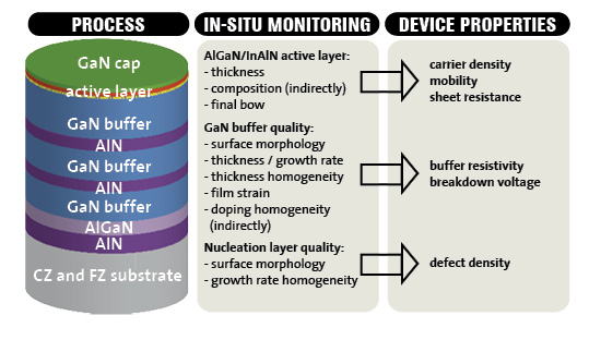
Laytec Power And Rf Electronics

A Fabrication Process Of The Algan Gan Hemt Structure B Download Scientific Diagram
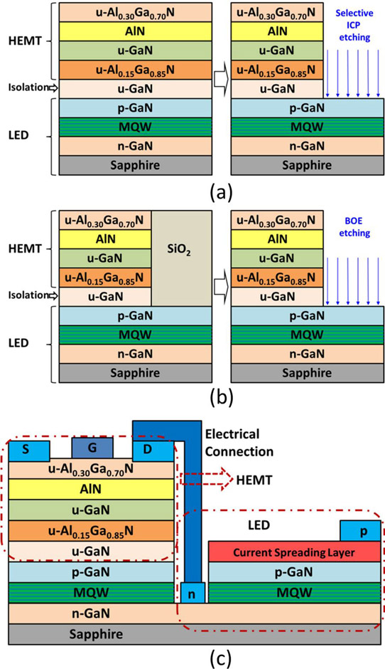
Monolithic Integration Of Nitride Semiconductor Hemts And Leds

A Fabrication Process Of The Algan Gan Hemt Structure B Download Scientific Diagram

High Electron Mobility Transistor Wikipedia
Effects Of Gate Shaping And Consequent Process Changes On Algan Gan Hemt Reliability Topic Of Research Paper In Materials Engineering Download Scholarly Article Pdf And Read For Free On Cyberleninka Open Science
Transphorm Gan On Silicon Hemt Tph36ps 16 Teardown Reverse Costin

Figure 3 From 0 1 M M Inp Hemt Mmic Fabrication On 100 Mm Wafers For Low Cost High Performance Millimeter Wave Applications Semantic Scholar
Molecular Gated Algan Gan High Electron Mobility Transistor For Ph Detection Analyst Rsc Publishing

A Fabrication Process Of The Algan Gan Hemt Structure B Download Scientific Diagram

Schematics Showing The Process Flow Of E D Mode Hemts A Ohmic Download Scientific Diagram
Tel Archives Ouvertes Fr Tel Document

High Rf Performance Enhancement Mode Al2o3 Algan Gan Mis Hemts Fabricated With High Temperature Gate Recess Technique Semantic Scholar
Electronics Free Full Text A Comprehensive Review Of Recent Progress On Gan High Electron Mobility Transistors Devices Fabrication And Reliability Html

Normally Off Hemt Device With Field Plates Power Microelectronics Device And Process Technologies

Schematic Views Of The Process Flow For Micro Trench Fabrication In Download Scientific Diagram

Process Flow For Fabrication Of Protected And Passivated Aln Gan Download Scientific Diagram

Figure 10 From A Gaas Soi Hemt Fabricated By Fluidic Self Assembly And Its Application To An Rf Switch Semantic Scholar
An Effective Hydroxylation Route For A Highly Sensitive Glucose Sensor Using Aptes Gox Functionalized Algan Gan High Electron Mobility Transistor Rsc Advances Rsc Publishing
Electronics Free Full Text A Comprehensive Review Of Recent Progress On Gan High Electron Mobility Transistors Devices Fabrication And Reliability Html
2

Figure 1 From Advantage Of Tin Schottky Gate Over Conventional Ni For Improved Electrical Characteristics In Algan Gan Hemt Semantic Scholar


