Hemt Pr
For PR measurements, a DC 3V tungsten halogen lamp was used as the white-light source, and a He-Ne laser (632.8 nm) acted as the modulation light source of the HEMT sample.
Hemt pr. Therefore, HEMT characterist controlled and as a result, any type of GaN can be fabricated. High Electron Mobility Transistors (HEMTs) Active Region Source DrainGate S. The products are used worldwide by major cutting-edge semiconductor device companies.
The epitaxial layers were grown on a 2-in Si (111) substrate by MOCVD. This is an important device for high speed, high frequency, digital circuits and microwave circuits with low noise applications. HEMT PR 03-6721-08.
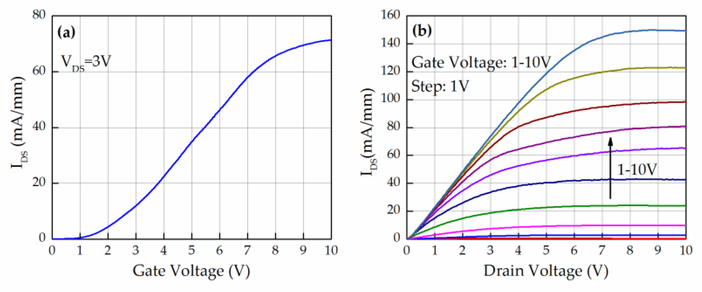
A heterojunction) as the channel instead of a doped region (as is generally the case for a MOSFET). Buffer Lg Wg 0 2 4 6 8 10 12 14 16 0 0 400 600 800 1000 g m = 0 mS/mm ∆∆∆∆V G = 1 V V G = 2 V I D (mA/mm) V DS (V) Open channel Pinch off Similar to normally-on MOSFETs but no substrate doping. The HEMT device exhibited improvement in the drain current, with a subtle decreasing tendency in the leakage current.
The system can't perform the operation now. Not wonder store 06-6110-5466. At high doses of γ-ray irradiation, the trends in the material and device.
The fabricated 1 μm long gate GaN HEMT, Pr 2 O 3 MIS-HEMT, and P 2 S 5 /(NH 4) 2 + UV-treated Pr 2 O 3 MIS-HEMT were tested on-wafer and the microwave power characteristics were evaluated using a load-pull system with automatic tuners, which simultaneously provides conjugate-matched input and load impedances for the maximum output power. High Voltage Vertical GaN-on-GaN Schottky Barrier Diode with High Energy Fluorine Ion Implantation Based on Space. TI provides gallium nitride (GaN) power devices and easy-to-use modules that meet next generation system requirements and TI's high standards of quality and reliability.
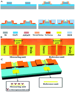
PR PR PR Sapphire Substrate Buffer GaN AlGaN ②Mask 02 –S/D Ø Sourceanddraincontactto AlGaN Ø Themetalmustbe depositedafteracompletely cleanprocesstoeliminate layersbetweenAlGaNand Metal A GaN-on-Sapphire HEMT Process Flow Example ③Deposit S/D metal Ø Deposit ohmic contacts on top of AlGaN as source and drain Sapphire Substrate Buffer. HEMT DC characteristics are set independe the resonator;. Our gallium nitride (GaN) HEMT epiwafer products are well known for their high breakdown voltage with low leakage current and excellent two dimensional electron gas (2DEG) characteristics.
Hemet is a city in the San Jacinto Valley in Riverside County, California, United States. This Time incよりCAMPINOXのデジカモショルダーバッグがhouyhnhnm.jp読者プレゼントになりました。詳しくは houyhnhnm.jp をご確認ください。 (締め切り12年5月16日). AlGaN/GaN High Electron Mobility Transistors (HEMT) on a (001)-oriented silicon (Si) substrate are fabricated.
The integrated power GaNs have R DS(ON) of 150 mΩ and 650 V drain‑source breakdown voltage, while the high side of the embedded gate driver can be easily supplied by the integrated bootstrap diode. HEMT PR, 東京都 渋谷区. The pr esent work focus on the m easurement of electron.
HEMT PR, 東京都 渋谷区. It covers a total area of 27.847 square miles (72 km2), about half of the valley, which it shares with the neighboring city of San Jacinto. / ノース ワークスのネックレス¥10,000(HEMT PR/tel03-6721-08) / ナラティブ・プラトゥーンのブレスレット¥9,500(ロジェ/tel042-316-3525) アットダーティーのベスト¥15,000、オーバーオール¥28,000、ドレスヒッピーのキャスケット¥8,000、.
For PR measurements, a DC 3 V tungsten-halogen lamp was the white-light source, and a He-Ne laser (632.8 nm) acted as the modulation light source of the HEMT sample. The MASTERGAN1 features UVLO protection on both the lower and upper driving sections, preventing the power switches from operating in low efficiency or dangerous conditions, and the interlocking. Hatto 登米無双』 - Duration:.
HEMT PRは、ファッションブランド、ファッションメーカーのPR及び ブランディングを行うPRオフィスです。 クリエイターの情熱を消費者へ伝える創造性豊かなプロモーション、 展示会やイベントに向けた構築的な販促企画を提案します。. AlGaN/GaN HEMT s ar e pr omising ca ndidates f or next genera tion microwa ve power am pli ers and high-vol tage switch es owing to their superior p roperties ,. The HEMT or High Electron Mobility Transistor is a type of field effect transistor (FET), that is used to offer a combination of low noise figure and very high levels of performance at microwave frequencies.
The name HEMT stands for High Electron Mobility Transistor. Johnbull Customer Center 050-3000-1038. 12 AUTUMN & WINTER よりスタートのFAHBLE(ファーブル)がeyescream.jp、Houyhnhnm Blogで紹介されています。.
In addition to the very high frequency performance, the HEMT also offers a very attractive low noise performance. Volíme vždy nejlepší materiál. This increase saturates at drain bias voltages above 50V.
Journal of Semiconductors 39 (7), 1-8, 18. UNITE NINE 03-5464-9976. HEMT PRは、ファッションブランド、ファッションメーカーのPR及びブランディングを行うPRオフィスです。クリエイターの情熱を消費者へ伝える想像性豊かなプロモーション、展示会やイベントに向けた構築的な販促企画を提案します。 HEMT PR tel 03-6427-1030 東京都渋谷区渋谷1-17-1 TOC第2ビル902.
HEMT PRは、ファッションブランド、ファッションメーカーのPR及び ブランディングを行うPRオフィスです。 クリエイターの情熱を消費者へ伝える創造性豊かなプロモーション、 展示会やイベントに向けた構築的な販促企画を提案します。. The report provides an estimation of. When the drain of the p-GaN HEMT is biased in the off-state the threshold voltage (Vth) shows a linear increase up to ∼ 40%.
249 Followers, 79 Following, 95 Posts - See Instagram photos and videos from HEMT PR (@hemt_pr). This study elucidates the praseodymium oxide (Pr 2 O 3)-passivated AlGaN/GaN metal–oxide–semiconductor high electron mobility transistors (MOS-HEMTs) with high dielectric constant, and with their AlGaN Schottky layers treated with P 2 S 5 /(NH 4) 2 S X + ultraviolet (UV) illumination. In accordance with Riverside County's limit on gatherings to 10 or less, and CA's Stay at Home Order, tonight's Council Meeting will be available through a conference line for public comments.
For instance, by simply GaN resonator input to the HEMT drain, formed, in which the resonance can be su addition of two capacitances connected to th configuration) 8. A high-electron-mobility transistor (HEMT), also known as heterostructure FET (HFET) or modulation-doped FET (MODFET), is a field-effect transistor incorporating a junction between two materials with different band gaps (i.e. JACK of ALL TRADES press room 03-3401-5001.
Dělíme svou výrobu mezi pilu zabývající se prvotním zpracováním dřeva s produkcí zejména stavebního řeziva a zakázkovou truhlárnu. Maojun Wang's 65 research works with 4 citations and 4,773 reads, including:. Jsme spolehlivým dodavatelem přes 30 let.
Small-signal model parameter extraction of E-mode N-polar GaN MOS-HEMT using optimization algorithms and its comparison. Craigslist provides local classifieds and forums for jobs, housing, for sale, services, local community, and events. HEMT has the required certification and manpower to repair, refurbish and service.
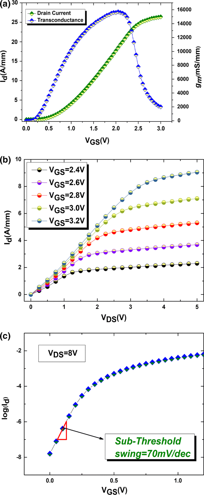
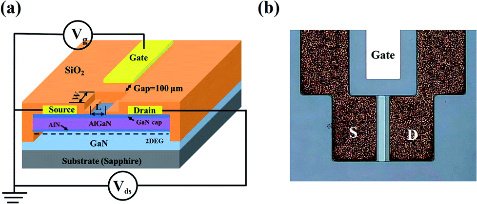
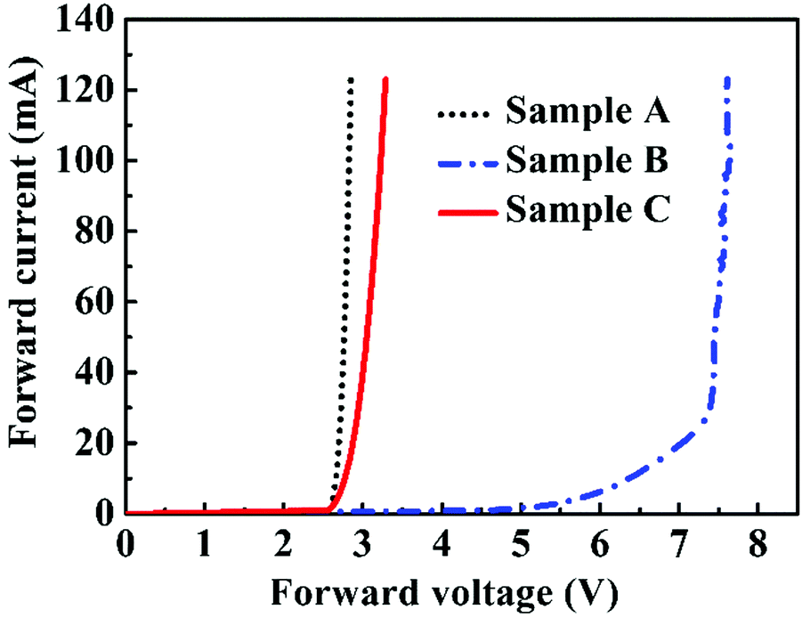
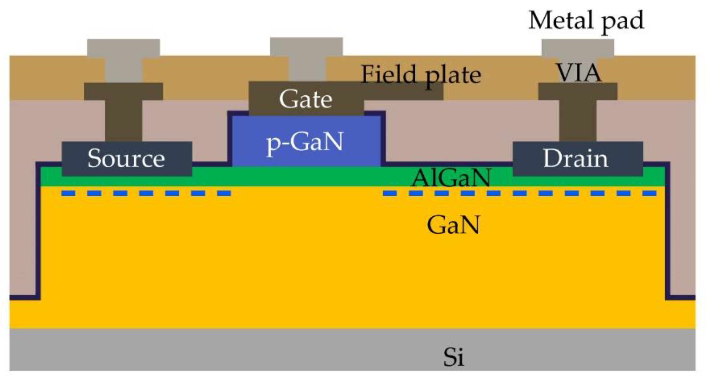
After the preparation of the epitaxial wafer, the normally-off p-GaN/AlGaN/GaN HEMT on a Si substrate was achieved by hydrogen plasma treatment .The main structure of the epitaxial wafer includes a 1 µm GaN buffer layer, a 100 nm GaN channel layer, a 1 nm AlN spacer layer, an 18 nm undoped Al 0.2 Ga 0.8 N barrier layer. GaN based high-electron mobility transistors (HEMT) are strong candidates for next generation electronics such as power amplifiers, broadbandcommunicationandhigh-voltageswitchesduetotheirhigh. Output power of 100 mW was the pump source.
Fabrication HEMT has a fully equipped fabrication shop, capable to carry out fabrication. HEMT with HZO dielectric shows an enhanced DC output performance with an increase of 54% at the optimal working condition, which is indeed much higher than that of the HfO2 MOS-HEMT (40%). The device with a gate.
The new GaN power HEMT, TDG650E60, is the highest voltage GaN power device available on the market for hi- rel military and space applications, and is now available with both top- or bottom-side cooled options. Barnstormerがhouyhnhnmの人気企画essentials vol.4 “authentic pants”で紹介されました。. Valves & Pumps HEMT is an approved DHV & CNV Valve repair shop.
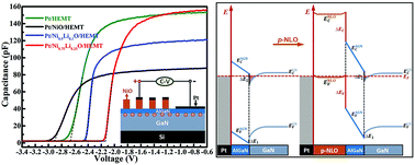
Buffer Lg Wg Active Region Source DrainGate S. And the HZO MOS-HEMT exhibits a higher Ion/Ioff ratio of 106, an excellent subthreshold swing (SS) of 85 mV/decade, and a. For PL measurements of the HEMT device, a frequency-doubled Nd:YAG laser (532 nm) with average output power of 100mW was used as the pump source.
Vyrábíme nábytek na zakázku. Measurements of an InGaAs/GaAs graded-channel HEMT have been carried out with this PL and PR system. Bukht16 Autumn & Winter CollectionがFashionsnapで公開されました。 「ブフト(bukht)」が発表した16-17年秋冬コレクションのテーマは「ONKO-CHISHIN」。.
An electron-beam evaporated Pr 2 O 3 insulator is used, instead of traditional plasma-assisted chemical. 12 AUTUMN & WINTER よりスタートのFAHBLE(ファーブル)がeyescream.jp、Houyhnhnm Blogで紹介されています。.
Characterization And Analysis Of Low Noise Gan Hemt Based Inverter Circuits Springerlink

Moscap And Hemt Process Flows A Moscap Process Flow N Gan Substrate Download Scientific Diagram
Egn010mk Eudyna High Voltage High Power Gan Hemt Html Datasheet
Hemt Pr のギャラリー

Moscap And Hemt Process Flows A Moscap Process Flow N Gan Substrate Download Scientific Diagram

Clf1g0035s 100 Hemt Datasheet Pdf Gan Hemt Equivalent Catalog

明日なに着てく Hemt Pr平山さんの休日はワイドシルエットでリラックス Fashion Uomo Webuomo

Hemt Pr Varde77

650 V Gan Fets Work With Low Cost Gate Drivers Edn
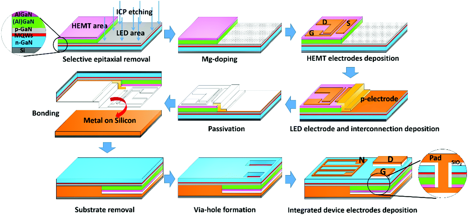
Efficiency Improved By Monolithic Integration Of Hemt With Vertical Structure Leds And Mg Doping On Dry Etched Gan Journal Of Materials Chemistry C Rsc Publishing

Schematic Views Of The Process Flow For Micro Trench Fabrication In Download Scientific Diagram

Surface States In Algan Gan High Electron Mobility Transistors Quantitative Energetic Profiles And Dynamics Of The Surface Fermi Level Applied Physics Letters Vol 115 No 2
Egn010mk Eudyna High Voltage High Power Gan Hemt Html Datasheet
Experimental Values Of The Intersubband Transition Energies From The In Download Table
Characterization And Analysis Of Low Noise Gan Hemt Based Inverter Circuits Springerlink
Http Www Nanoscience Gatech Edu Paper 1 S2 0 S Main Pdf

Hemt Pr Mastered
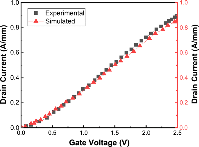
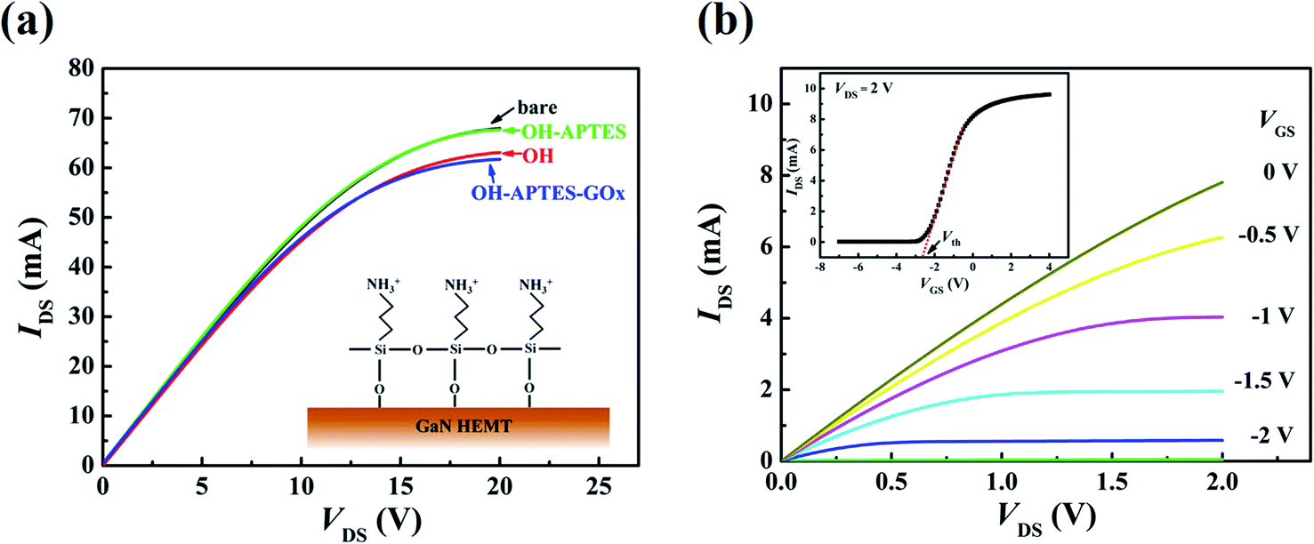
An Effective Hydroxylation Route For A Highly Sensitive Glucose Sensor Using Aptes Gox Functionalized Algan Gan High Electron Mobility Transistor Rsc Advances Rsc Publishing Doi 10 1039 C9raf

Schematic Views Of The Process Flow For Micro Trench Fabrication In Download Scientific Diagram
Http Www Jsts Org Html Journal Journal Files 19 12 Year19volume19 06 04 Pdf

Gan Lattice Matched Zno Pr2o3 Film As Gate Dielectric Oxide Layer For Algan Gan Hemt Semantic Scholar

Color Online Flowchart Of Backside Processing Of The Gan Hemt On A Download Scientific Diagram

一週間スナップ 4 平山洋次 Hemt Pr ディレクター 4月21日 土 分 Mastered

Design And Analysis Of 10 Nm T Gate Enhancement Mode Mos Hemt For High Power Microwave Applications Sciencedirect

Transphorm Releases Industry S First Jedec Qualified 600v Gan Hemt

Uomomagazine 平山洋次さん 39歳 Hemt Pr ディレクター ボルドーはこれから注目のカラーという体感もあって 気分ですね という平山さん 今日着用のスニーカー Wacoca

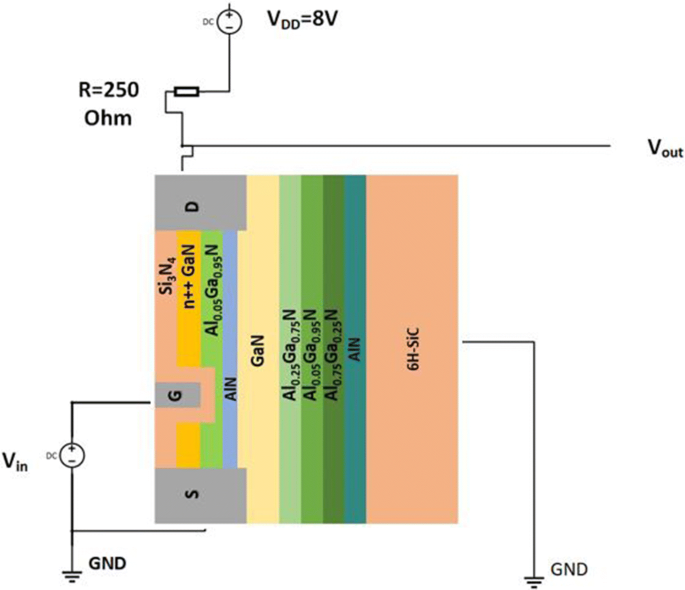
New Gan Based Hemt With Si3n4 Or Un Doped Region In The Barrier For High Power Applications Sciencedirect
Characterization And Analysis Of Low Noise Gan Hemt Based Inverter Circuits Springerlink
Www Osti Gov Servlets Purl
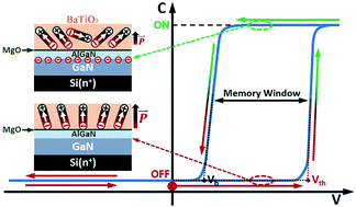
Strong Interfacial Coupling Effects Of Ferroelectric Polarization With Two Dimensional Electron Gas In Batio3 Mgo Algan Gan Si Heterostructures Journal Of Materials Chemistry C Rsc Publishing
Al Gan Aln Gan Sic Hemt Structure With High Mobility Gan Thin Layer A
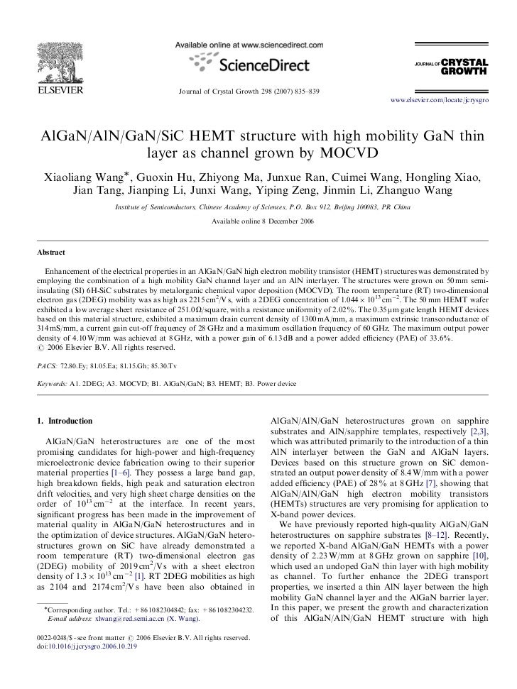
Design Principle For A P Type Oxide Gate Layer On Algan Gan Toward Normally Off Hemts Li Doped Nio As A Model Journal Of Materials Chemistry C Rsc Publishing

People Reebok Classic Houyhnhnm Re Mag

Figure 9 Gan Based High K Praseodymium Oxide Gate Misfets With Uv Interface Treatment Technology

明日なに着てく Hemt Pr平山さんの休日はワイドシルエットでリラックス Fashion Uomo Webuomo
Gan On Sic Hemt Transistor Igt5259l50 18 04 17 Microwave Journal

Improved Gate Close To Source Structure For A Gan Hemt Download Scientific Diagram

Recess Etch For Hemt Application Ppt Download
Osa Practical Photoluminescence And Photoreflectance Spectroscopic System For Optical Characterization Of Semiconductor Devices

Gan Power Hemt Tutorial Gan Basics Pdf Free Download

Hemt Research Papers Academia Edu
Stars Library Ucf Edu Cgi Viewcontent Cgi Article 7690 Context Etd
Www Osti Gov Servlets Purl

Wolfspeed S Next Generation Gan Hemts Deliver Unmatched Efficiency 17 09 14 Microwave Journal

Design And Analysis Of 10 Nm T Gate Enhancement Mode Mos Hemt For High Power Microwave Applications Sciencedirect

Gan Lattice Matched Zno Pr2o3 Film As Gate Dielectric Oxide Layer For Algan Gan Hemt Semantic Scholar
Photoluminescence And Photoreflectance Analysis Of Semiconductor Devices Horiba

明日なに着てく Hemt Pr平山さんの休日はワイドシルエットでリラックス Youtube

New Gan Based Hemt With Si3n4 Or Un Doped Region In The Barrier For High Power Applications Sciencedirect
Http Www Nanoscience Gatech Edu Paper 1 S2 0 S Main Pdf

Pdf Reliability Of Gan Based Hemt Devices

Hemt Pr Facebook

Design And Analysis Of 10 Nm T Gate Enhancement Mode Mos Hemt For High Power Microwave Applications Sciencedirect

Clf1g0035s 100 Hemt Datasheet Pdf Gan Hemt Equivalent Catalog
Http Www Jsts Org Html Journal Journal Files 19 12 Year19volume19 06 04 Pdf

Gan Hemt Mmic With Integrated Class G Switching Stage For Discrete Level Supply Modulation For Ghz Space Applications Semantic Scholar

一週間スナップ 4 平山洋次 Hemt Pr ディレクター 4月18日 水 分 Mastered
Efficiency Improved By Monolithic Integration Of Hemt With Vertical Structure Leds And Mg Doping On Dry Etched Gan Journal Of Materials Chemistry C Rsc Publishing

Gan Lattice Matched Zno Pr2o3 Film As Gate Dielectric Oxide Layer For Algan Gan Hemt Semantic Scholar

Study On Small Signal Modeling Of Gan Hemt Devices

Gan Based High K Praseodymium Oxide Gate Misfets With Uv Interface Treatment Technology
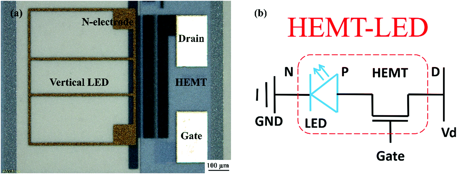
Efficiency Improved By Monolithic Integration Of Hemt With Vertical Structure Leds And Mg Doping On Dry Etched Gan Journal Of Materials Chemistry C Rsc Publishing
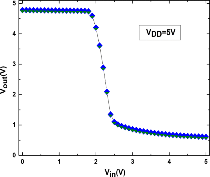
Characterization And Analysis Of Low Noise Gan Hemt Based Inverter Circuits Springerlink

一週間スナップ 4 平山洋次 Hemt Pr ディレクター 4月22日 日 分 Antenna アンテナ

Hemt Pr

4 4 Yield Enhancement Of 0 25 M Gan Hemt Pure Play Gan Foundry 0 25mm Hemt Technology For Rf Applications Monterey California U S A Ieee Csic Symposium Oct 6 Pdf Document
Research Information Bris Ac Uk Files Full Text Pdf Final Published Version Pdf
Electronics Free Full Text A Comprehensive Review Of Recent Progress On Gan High Electron Mobility Transistors Devices Fabrication And Reliability Html
Electronics Free Full Text A Comprehensive Review Of Recent Progress On Gan High Electron Mobility Transistors Devices Fabrication And Reliability Html

Hemt Pr
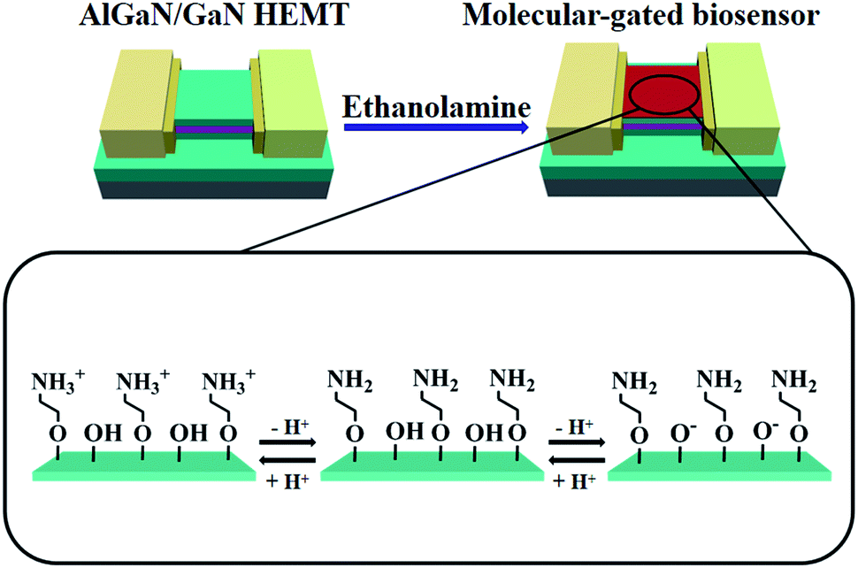
Highly Sensitive Algan Gan Hemt Biosensors Using An Ethanolamine Modification Strategy For Bioassay Applications Rsc Advances Rsc Publishing

Hemt Pr 平山 洋次 Yooochang Twitter

Cree 12ghz Gan Hemt Based Mmics Now At Mouser Puerto Rico

Algan Gan Based Saw Hemt Devices For Chemical Gas Sensors Operating In Ghz Range Pdf Document
Device Performance Of An As Fabricated P Gan E Hemt A Transfer Download Scientific Diagram
Http Www Xidian Edu Cn Hyjsktz Docs Pdf

High K Praseodymium Oxide Passivated Algan Gan Mosfets Using P2s5 Nh4 2sx Uv Interface Treatment Sciencedirect

Hemt Pr

Hemt Pr サンプルセール 詳細になります ヘムト日記 平山洋次 Shop Brand Blog ショップ ブランドブログ Houyhnhnm フイナム
Characterization And Analysis Of Low Noise Gan Hemt Based Inverter Circuits Springerlink
Electronics Free Full Text A Comprehensive Review Of Recent Progress On Gan High Electron Mobility Transistors Devices Fabrication And Reliability Html

Hemt Pr Facebook
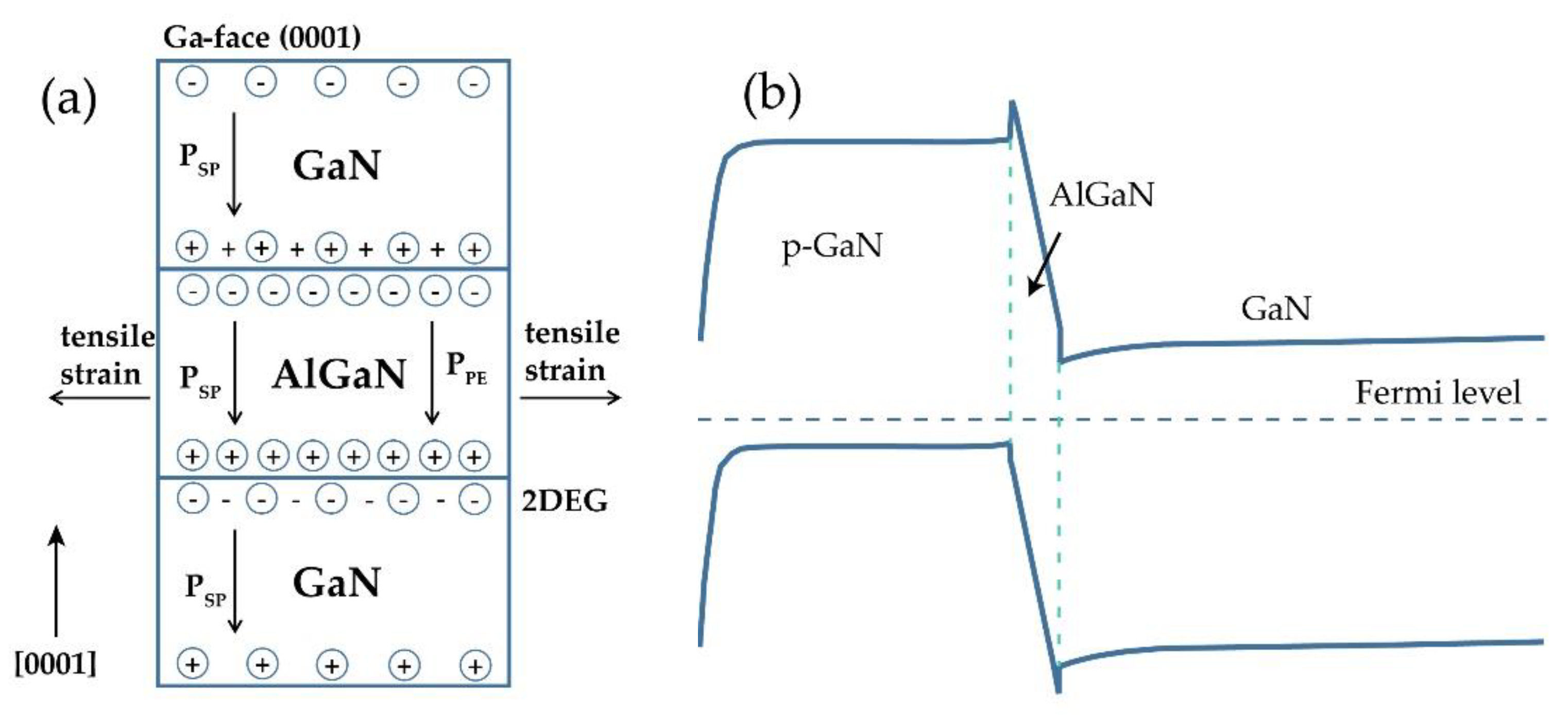
Investigation Of Algan Gan High Electron Mobility Transistor Structures On 0 Mm Silicon 111 Substrates Employing Different Buffer Layer Configurations Scientific Reports

Hemt Pr 取扱い開始 Dr Franken

Hemt Pr Old Parkのデニムセットアップ Sevenhomme オールドパーク Facebook
Http Www Xidian Edu Cn Hyjsktz Docs Pdf
Characterization And Analysis Of Low Noise Gan Hemt Based Inverter Circuits Springerlink

Color Online Pr Thin Red Lines And Cer Thick Lines Spectra Of Download Scientific Diagram

Large Periphery Gan Hemts Modeling Using Distributed Gate Resistance Hassan 19 Physica Status Solidi A Wiley Online Library
Http Trace Tennessee Edu Cgi Viewcontent Cgi Article 4269 Context Utk Graddiss

Viscosity Dependent Drain Current Noise Of Algan Gan High Electron Mobility Transistor In Polar Liquids Journal Of Applied Physics Vol 114 No
Ieeexplore Ieee Org Iel5 16 Pdf
Stars Library Ucf Edu Cgi Viewcontent Cgi Article 7690 Context Etd

一週間スナップ 4 平山洋次 Hemt Pr ディレクター 4月16日 月 分 Mastered

Pdf Stability Of Submicron Algan Gan Hemt Devices Irradiated By Gamma Rays Goran Ristic Academia Edu
2

New Gan Based Hemt With Si3n4 Or Un Doped Region In The Barrier For High Power Applications Sciencedirect
Http Www Xidian Edu Cn Hyjsktz Docs Pdf
A Differential Extended Gate Algan Gan Hemt Sensor For Real Time Detection Of Ionic Pollutants Analytical Methods Rsc Publishing
Electronics Free Full Text A Comprehensive Review Of Recent Progress On Gan High Electron Mobility Transistors Devices Fabrication And Reliability Html
An Effective Hydroxylation Route For A Highly Sensitive Glucose Sensor Using Aptes Gox Functionalized Algan Gan High Electron Mobility Transistor Rsc Advances Rsc Publishing Doi 10 1039 C9raf


